We have already learned earlier, but it is much more interesting to control this process using buttons, and the LED garland will serve as a good visual example.
Connecting a button to a microcontroller
The garland diagram is shown below.

When a button (key) is connected to a microcontroller, the corresponding MK pin must be configured as an input. In this case, the microcontroller will constantly read the state, or rather the potential level at this pin. Therefore, the program algorithm can be constructed in such a way that if at a certain pin of the MK the potential changes from high to low or vice versa, then a certain action will be performed, for example, an LED will light up.
To configure certain pins of the MK as input, zeros should be written to the corresponding bits of the DDR register. By the way, if the MK pins are not used, then it is also recommended to configure them for input. Since we will only connect buttons to port B, we will write all zeros to the DDRB register with the following command:
DDRB = 0b00000000;
When a microcontroller pin is configured as an input, it can initially be in two states, which are set using the PORT register.

If the PORT register bit is set to zero, then the pin has a high input impedance.
When the bit is set to one, a pull-up resistor is connected to the MK pin. The resistor is so called because through it a high potential (+ 5 V) is “pulled up” to the corresponding point in the electrical circuit; in this case - to the pin of the microcontroller.
Checking the status of the MK output using PINx
To know at any time what potential is present at the pin, you should check (read) the corresponding bit in the PIN register.
By analogy, this register can be compared to a sensor. You can only read information from it. You can't write anything to it. PIN is the opposite of the PORT register, which only writes to, but does not read, data.
It is more preferable to set the PORT register to one, i.e. use of internal pull-up resistor MK. This option has significant noise immunity, since to change the high potential to a low one, the output must be directly connected to ground or a common wire.
If the pin is made with a high input impedance, then any more or less powerful electromagnetic interference can induce a certain potential on it that exceeds specific value and the microcontroller will perceive the interference as a change from low potential to high. Therefore, in our program we will use an internal pull-up resistor.
We connect one contact of the key to ground (common wire), and the second to the pin of the microcontroller. When the key is open, the output is at a high potential (+ 5 V), pulled up by the internal resistor of the MK. In this case, the corresponding bit of the PIN register will be set to one.
When you press the button, this pin will connect to the common wire (“minus”) and a low potential will appear on it. And the PIN register bit will automatically be set to zero.
Please note that the pull-up resistor also protects the circuit from a short circuit when the button is pressed.
LED garland in code
Now let's write the entire program code and then look at it individual elements. The algorithm of the program is as follows: when the first key is closed, the “lights” will turn on in one sequence, and when the second is closed, the “lights” will light up differently. If both buttons are pressed, then all LEDs should be off.
#define F_CPU 1000000UL // Declare the operating frequency of the microcontroller 1 MHz
#include
#include
#define Z 300 // Name the delay value Z
#define VD PORTD // Assign the name VD to port D
#define K PORTB // Assign the name K to port B, to which the buttons are connected
int main(void)
DDRB = 0b00000000; // Configure port B for input
DDRD = 0b11111111; // Configure port D for output
VD = 0b00000000; // Turn off all lights
K = 0b11111111; // Turn on pull-up resistors
while (1)
if (PINB == 0b11111110) // Check if the 1st button is pressed
VD = 0b11111111; // If the key is closed, then we flash the “lights”
_delay_ms(Z);
VD = 0b00000000;
_delay_ms(Z);
else
VD = 0b00000000; // If the key is open, then all LEDs are turned off
if (PINB == 0b11111101) // Check if the 2nd button is pressed
VD = 0b00000001; // If the button is pressed, then turn on the LED one by one
_ delay_ ms(Z); // with a delay of 0.3 s
VD = 0b00000011;
_delay_ms(Z);
VD = 0b00000111;
_delay_ms(Z);
VD = 0b00001111;
_delay_ms(Z);
LED = 0b00011111;
_delay_ms(Z);
VD = 0b00111111;
_delay_ms(Z);
VD = 0b01111111;
_ delay_ms(Z);
VD = 0b11111111;
_delay_ms(Z);
VD = 0b00000000;
_ delay_ ms(Z);
else
VD = 0b00000000; // If the key is not closed, then all LEDs are turned off
Operators if And else
The purpose of preprocessors and them are well known from previous articles. What's new to us here is the if statement. If is translated from English as “if”. If the condition specified in parentheses is met, i.e. true, then the program code inside the curly braces is executed. For example, if variable a is greater than 1 unit, then variable c will be assigned the value a + b.
if (a >1)
c = a + b;
Otherwise, when the value of a is less than or equal to one, the program code in the curly braces will not be executed.
If only one command is executed in curly braces, then the C syntax allows you to simplify the notation and do without curly braces:
if (a >1) c = a + b;
The if statement also works in conjunction with the else statement.
if (a >1) → if a >1, then = a + b
c = a + b;
else → otherwise, c = a - b
c = a - b;
It works like this. If a > 1, then c = a + b. Otherwise, i.e. when a is less than or equal to one, then c = a – b.
Explanation of the program code
Now let's return to our program. If the button connected to PB0 is pressed, then a low potential appears on the pin and the corresponding bit of the PINB register is set to zero. In this case, the condition in curly brackets will be fulfilled, i.e. the garland will start flashing.
Note that the assignment command consists of one equal sign "=", and the command to test the condition "equals" consists of two equal signs written without a space "==".
When the button is not pressed, the PINB register bit will show a one caused by the pull-up resistor being high. In this case, control will pass to the else statement and all LEDs will be turned off.
When the second key is closed, the output of which is connected to port PB1, the second program code will be executed, and the LEDs will begin to turn on one by one with a time delay of 0.3 seconds.
Thus, a garland on a microcontroller can contain a different number of LEDs and keys. Moreover, for each closing or opening of the key contacts, you can prescribe your own algorithm for the operation of the garland.
It can also be controlled with just one button. This option has a slightly more complicated code, and we will consider it in a separate article. There we will also look at how to connect powerful LEDs to the MK.

Earlier in the article, you looked in detail at setting up the output, and here - for the input. Now let's put everything together and present a simple visual algorithm.
This SDS is developed in two versions. The first controls only the LEDs located on its board and is intended for developing and debugging lighting effects programs. A microcontroller with a debugged program can be transferred to the board of the second version of the SDU, to which you can connect 16 lighting devices powered from a 220 V network
Of the 20 pins of the ATtiny2313 microcontroller, 19 are used in the SDS under consideration: two for supplying the supply voltage; one - for connecting a button that controls the speed of playback of lighting effects; 16 - for generating control signals for garlands or other lighting devices.
There are eight effects playback speed settings; they can be switched in a circle by pressing a button. At minimum speed, the state of the garlands changes every 8 s, and at maximum speed, the change period is reduced to 0.5...1 s. It should be borne in mind that due to the nature of the program, the duration of pressing the button required to switch the speed is quite long. In addition, it depends on the speed currently set. The microcontroller stores speed information in its EEPROM, so when the SDU is turned on, it becomes the same as it was in the previous operating session.
Rice. 1. SDU circuit with ATtiny2313 microcontroller for 16 garlands
The circuit diagram of the debug version of the SDU, which controls only LEDs HL1-HL16, is shown in rice. 1.
Microcontroller DD1 operates from an internal RC oscillator with a frequency of 4 MHz. The XP1 connector is intended for connection to the programmer of a microcontroller installed in the SDU panel. During programming, the LED power supply circuit must be broken by switch SA1, which eliminates their influence on the programming process. Resistor R1 maintains a high logic voltage level at the PD2 input of the microcontroller when the SB1 button is released. When the button is pressed, this level goes low.
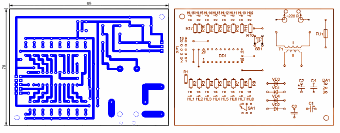
The device is assembled on a printed circuit board measuring 95x70 mm made of foil fiberglass. Its drawing is shown in rice, 2. There is a panel on the board for the microcontroller. This allows you to program it and test it in operation, and then transfer it to another SDS, which will be described below.
The board is designed to install oxide capacitors (C1 and C2) SR or similar. The dielectric of capacitors SZ and C4 is ceramic. Resistors - CF-0.125 or other similar ones. Transformer T1 - TPG-2 with a secondary alternating voltage of 6 V, designed for installation on a printed circuit board. You can use its analog BVEI 306 2061 with a power of 2.6 VA. In the case under consideration, the DA1 stabilizer does not require a heat sink. Buttons SB1 and switch SA1 can be of any size suitable for installation on the board.
The second version of the SDU controls not LEDs, but incandescent lamps or other 220 V lighting devices. To do this, each of the resistor-LED pairs of the previous version is replaced by a triac switch, the circuit of which is shown in rice. 3. To control the powerful triac VS1, optocoupler 1)1 is used here, the photodinistor of which is designed so that the moments of its opening always coincide with the transitions of the voltage applied to it through zero. This reduces the electromagnetic interference generated by the SDU.
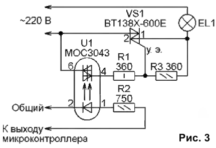
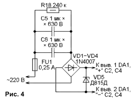
Since only 5 mA of current through its emitting diode is sufficient to control the MOS3043 optocoupler, the total load on the microcontroller does not exceed 80 mA. The total current consumption from the power supply in the new version is approximately two times less. This made it possible to abandon the transformer and use a transformerless unit with quenching capacitors. On his diagram ( rice. 4) the numbering of elements continues what started on rice. 1.
The printed circuit board of the second option has dimensions of 195x85 mm. Its drawing is shown in rice. 5. Elements of sixteen identical switches have position numbers on it with digital prefixes indicating the serial number of the switch. For example, 8R1—8R3, 8U1, 8VS1 are the elements of the eighth switch, which replaced resistor R9 and LED HL8 and controls an incandescent lamp (or a garland assembled from them) 8EL1.

All 16 triacs 1VS1 - 16VS1 are mounted on a common heat sink made of an aluminum plate with dimensions of 160x25x2 mm, located perpendicular to the surface of the board. Mounting holes for triacs are drilled in it at a height of 19 mm from the board.
Triacs VT138X-600 in a fully insulated TO-220F housing can be replaced by devices of the VT137-VT139 series for 600 or 800 V, including those in a conventional TO-220 housing with a metal mounting and heat-dissipating flange. Since this flange is connected inside the triac to its pin 2, and all these pins are connected on the board, insulating the triacs from the heat sink is not required.
It is recommended to first attach the triacs to the heat sink, and then mount their entire assembly on the board. Resistors 1R3-16R3 are soldered directly to the triac terminals. Pins 1 of the triacs are clamped in the holes of the ZVI-10-2.5-6 mm2 screw terminals facing them, the block with which ( rice. 6) is installed along the long side of the board next to the triacs. There are a total of 17 pairs of clamps in the block, 16 of which are used to connect lamps 1EL1-16EL1, and another one is for their common wire.

Capacitors C5 and C6 - K73-17V or imported, capable of operating at an alternating voltage of at least 250 V. Resistors 1R1 - 16R1 - MF-1.
The microcontroller must have a panel in which it must be installed already programmed.
Attached to the article are three versions of the microcontroller program, suitable for use in both versions of the CDS:
PG16H_S_REGULhex - 16 garlands work independently;
PG8_MK_S_REG.hex - two groups of eight garlands work synchronously;
PG4_MK_S_REGUL.hex - four groups of four garlands work synchronously.
The microcontroller configuration is in all cases left set at the factory.
If a smaller number of garlands (LEDs) are used, then elements related to unused garlands may not be installed on the boards of the described SDS. When working with the SDS of the second option, all components of which have a galvanic connection to the network, it is necessary to comply with electrical safety rules.
Radio Magazine, No. 11 2014 I. ABZELILBASH, Sibay, Bashkiria
CMU/SDU on a microcontroller (8 channels)
This device combines a color music device (CMU) and a light dynamic device (SDU) with 8 channels, with many lighting effects. The outputs of the device are designed to connect a sufficiently powerful load.
Frequency separation among DMU channels is purely software and very simple; a PIC microcontroller PIC16F628A is used. The number of timer/counter pulses for a strictly defined period of time is counted and, depending on the value of this counter, one or another LED turns on.
And here is the diagram of the device:

Digging allows:
- Select mode - CMU/SDU. In the SDU mode, even if there is a signal at the input, only the main program of the light-dynamic device works. In the CMU mode, if there is no signal, the selected SDU effect is played as a background mode.
- Select the SDU effect. The button cyclically switches all possible effects of the dynamic light device.
- Increase and decrease speed. These buttons control the speed of the SDS effects; they have no effect on the CMU.
The printed circuit board is single-sided and quite simple. The LEDs installed on the board are debugging and serve simply as an additional visualization device.
For colored spotlights, I used ready-made spotlights from a hardware store. From them I removed the standard light bulb socket and installed a matrix of 37 bright LEDs there. Each spotlight has its own color - red, green, blue, etc., whatever we could find. Spotlights are placed at the corners of the room and at the midpoints at the top of the walls, all aimed at the center of the room. At night with music it looks very impressive, especially the strobe effect
2, diagram
This LED garland project on a microcontroller is well suited for beginners. The circuit is distinguished by its simplicity and contains a minimum of elements.
This device controls 13 LEDs connected to the microcontroller ports. An ATMEL microcontroller is used as a microcontroller: ATtiny231320PI. Thanks to the use of an internal oscillator, pins 4 and 5 are used as additional ports of the microcontroller PA0, PA1. The circuit provides the execution of 12 effect programs, 11 of which are individual combinations, and the 12th program is a sequential one-time repetition of previous effects. Switching to another program is done by pressing the SB1 button. Effect programs include running single fire, increasing fire, running shadow and much more.

The device has the ability to adjust the speed of changing combinations when executing a program, which is carried out by pressing the buttons: SB2 - increase speed and SB3 - decrease speed, provided that switch SA1 is in the "Program speed" position. It is also possible to adjust the frequency of LED lighting (from a stabilized glow until light flickering), which is carried out by pressing the buttons: SB2 - decrease (to flicker) and SB3 - increase, provided that switch SA1 is in the "Flicker frequency" position. For switch SA2, the closed position corresponds to the mode for adjusting the speed of program execution, and the open position corresponds to the mode for adjusting the frequency of LED lighting.
The numbering order of the LEDs in the circuit corresponds to their lighting order during program execution. If necessary, the RESET pin can be used for reset, but it is not used as the PA2 port. When programming, the device selected a clock frequency of 8 MHz from the internal oscillator (fuses CKSEL3..0 - 0100). Although it is possible to use a frequency of 4 MHz (fuses CKSEL3..0 - 0010) with corresponding changes in the time intervals of the circuit.
The type of LEDs indicated in the diagram was used in a prototype; any LEDs with a supply voltage of 2-3 volts are suitable for the circuit; resistors R1-R17 can be used to adjust the brightness of the LEDs.

You can download the HEX firmware, as well as the program files in assembler, below
List of radioelements
| Designation | Type | Denomination | Shop | ||
|---|---|---|---|---|---|
| DD1 | MK AVR 8-bit | ATtiny2313 | 1 | Search in store | |
| C1 | Electrolytic capacitor | 100 µF 10 V | 1 | Search in store | |
| R1-R17 | Resistor | 1 kOhm | 17 | Search in store | |
| LED1-LED13 | Light-emitting diode | LD571 | 13 | Search in store | |
| SB1-SB3 | Button | 3 | Search in store | ||
| SA1 | Switch | 1 | Search in store |
3, diagram
Christmas tree garland switch based on PIC16C84.

2. Device capabilities. Provides a choice of one of sixteen control programs (however 3. Device management.
"<<" - выбор программы, переключиться на предыдущую; In addition, when you turn on the device, you can select additional options. 4. Design and details. The design has galvanic contact with the network, so the metal "Advanced" users can try to improve the controls |
As people say - prepare your sleigh in the summer...
Surely on New Year You decorate the Christmas tree with all sorts of garlands, and most likely they have long since become boring with the monotony of their blinking. I would like to do something so that, wow, it blinks just like on the capital’s Christmas trees, only on a smaller scale. Or, as a last resort, hang it on the window so that this beauty illuminates the city from the 5th floor.
But alas, there are no such garlands for sale.
Actually, this is exactly the problem that had to be solved two years ago. Moreover, due to laziness, 2 years passed from idea to implementation, as usual, and everything was done in the last month. Actually, you will have more time (or I don’t understand anything about human psychology, and everything will be done exactly the same in the last 2 weeks before the new year?).
The result is a fairly simple design of individual modules with LEDs, and one common one that transmits commands from the computer to the network of these modules.
The first version of the module was conceived to connect them to the network via two wires, so that there would be less confusion and all that - but it didn’t work out; in the end, a fairly powerful and high-speed switch was required to switch the power of even a small number of modules - an obvious overkill for simplicity of design, so I gave preference the third wire is not so convenient, but it is much easier to organize a data transmission channel.
How everything works.

The developed network is capable of addressing up to 254 slave modules, which will be further called SLAVE - they are connected by only 3 wires, as you guessed - two wires are +12V power supply, common and the third is signal.
they have a simple scheme: 
As you can see, it supports 4 channels - Red, Green, Blue and Violet.
True, according to the results of practical testing, purple is clearly visible only close up, but how! Also, due to the fact that the colors are located too far from each other, the color mixing can only be seen from 10 meters away, if you use RGB LEDs the situation will be somewhat better.
In order to simplify the design, we also had to abandon quartz stabilization - firstly, the extra output takes away and secondly the cost quartz resonator quite noticeable and thirdly - there is no urgent need for it.
A protective cascade is assembled on the transistor so that the controller port is not knocked out by static - the line can still be quite long, in extreme cases only the transistor will suffer. The cascade is calculated in MicroCap and has an approximate response threshold of about 7 volts and a weak dependence of the threshold on temperature.
Naturally, in the best traditions, all modules respond to address number 255 - this way you can turn them all off at the same time with one command.
A module called MASTER is also connected to the network - it is an intermediary between the PC and the network of slave SLAVE modules. Among other things, it is a source of reference time for synchronizing slave modules in the absence of quartz stabilization in them.
Scheme: 
The circuit contains optional potentiometers - they can be used in a program on a PC for convenient and quick setup of the desired parameters, on this moment this is implemented only in the test program in the form of the ability to assign any of the potentiometers to any of the 4 channels. The circuit is connected to a PC via a USB-UART interface converter on an FT232 chip.
An example of a packet sent to the network: 
Its beginning: 
Electrical characteristics of the signal: log.0 corresponds to +9...12V, and log.1 corresponds to 0...5V.
As you can see, data is transmitted sequentially, at a fixed speed of 4 bits. This is due to the necessary margin for error in the data reception speed - SLAVE modules do not have quartz stabilization, and this approach guarantees data reception when the transmission speed deviates up to +-5% in excess of those that are compensated programmatic method based on measuring a calibrated interval at the beginning of data transmission, which provides resistance to reference frequency drift by another +-10%.
Actually, the algorithm of operation of the MASTER module is not so interesting (it is quite simple - we receive data via UART and forward it to the network of slave devices), all the most interesting solutions are implemented precisely in SLAVE modules, which actually allow you to adapt to the transmission speed.
The main and most important algorithm is the implementation of a 4-channel 8-bit software PWM which allows you to control 4 LEDs with 256 gradations of brightness for each of them. The implementation of this algorithm in hardware also determines the data transfer rate on the network - for software convenience, one bit is transmitted for each step of PWM operation. A preliminary implementation of the algorithm showed that it runs in 44 clock cycles, so it was decided to use a timer configured to interrupt every 100 clock cycles - this way, the interrupt has time to be guaranteed to be executed before the next one and execute part of the code of the main program.
At the selected clock frequency of the internal oscillator of 4.8 MHz, interrupts occur at a frequency of 48 kHz - this is the bit speed the network of slave devices has and the PWM is filled at the same speed - as a result, the frequency of the PWM signal is 187.5 Hz, which is quite enough not to notice the flickering of the LEDs. Also, in the interrupt handler, after executing the algorithm responsible for generating PWM, the state of the data bus is recorded - it turns out approximately in the middle of the timer overflow interval, this simplifies data reception. At the beginning of receiving the next 4-bit packet, the timer is reset, this is necessary for more precise synchronization reception and resistance to reception speed deviation.
The result is the following picture: 
The implementation of the algorithm for adjusting the transmission speed is interesting. At the beginning of the transmission, MASTER issues a pulse with a duration of 4 bits of log.0, from which all slave modules determine the required reception speed using a simple algorithm:
LDI tmp2, st_syn_delay DEC tmp2 ;<+ BREQ bad_sync ; | SBIC PINB, cmd_port; | RJMP PC-0x0003 ;-+
St_syn_delay = 60 - a constant that determines the maximum duration of the starting pulse, which is taken to be approximately 2 times the nominal value (for reliability)
Using an experimental method, the following dependence of the resulting number in tmp2 was established when the clock frequency deviates from the nominal:
4.3Mhz (-10%) 51 units (0x33) corresponds to 90 timer clocks to return the reception speed to nominal
4.8Mhz (+00%) 43 units (0x2B) - corresponds to 100 timer clocks (nominal)
5.3Mhz (+10%) 35 units (0x23) - corresponds to 110 timer clocks to return the reception speed to nominal
Based on these data, the correction factors for the timer interrupt period were calculated (this is how the reception speed is adjusted to the existing clock frequency of the controller):
Y(x) = 110-x*20/16
x = tmp2 - 35 = (0, 1, 2, 3, 4, 5, 6, 7, 8, 9, 10, 11, 12, 13, 14, 15, 16)
Y(x) = (110, 108.75, 107.5, 106.25, 105, 103.75, 102.5, 101.25, 100, 98.75, 97.5, 96.25, 95, 93.75, 92.5, 91.25, 90)
The numbers are rounded to whole numbers and stored in the EEPROM.
If, when applying voltage to the module, hold the line in the logical state “1”, a calibration subroutine will be activated, which will allow you to measure the period of the PWM signal with a frequency meter or oscilloscope without correction and, based on the measurements, judge the deviation of the clock frequency of the module controller from the nominal one, with a strong deviation of more than 15% The built-in RC oscillator calibration constant may need to be adjusted. Although the manufacturer promises calibration at the factory and deviation from the nominal value of no more than 10%.
At the moment, a Delphi program has been developed that allows you to reproduce a previously compiled pattern for 8 modules at a given speed. As well as a utility for working with a separate module (including reassigning the module address).
Firmware.
for the SLAVE module, only fuses CKSEL1 = 0 and SUT0 = 0 need to be flashed. The rest should be left unflashed. The contents of the EEPROM are flashed from the file RGBU-slave.eep, if necessary, you can immediately set the desired address of the module on the network - the 0th byte of the EEPROM, by default it is flashed as $FE = 254, address 0x13 contains the calibration constant of the built-in RC oscillator of the controller, at a frequency of 4.8 MHz it does not load automatically, so it is necessary to read the factory calibration value with the programmer and write it in this cell - this value is individual for each controller; with large frequency deviations from the nominal value, you can change the calibration through this cell without affecting the factory value.
For the MASTER module, it is necessary to flash only fuses SUT0 = 0, BOOTSZ0 = 0, BOOTSZ1 = 0, CKOPT = 0. Leave the rest unflashed.
Finally, a small demonstration of the garland located on the balcony:
In fact, the functionality of the garland is determined by the program on the PC - you can create color music, stylish iridescent room lighting (if you add LED drivers and use powerful LEDs) - etc. What do I plan to do in the future? The plans include a grid of 12 modules with 3-watt RGB LEDs, and room lighting based on pieces of 12-volt RGB tape (you only need field-effect transistors for switching the tape for each module, 3 pieces or 4 if you add a piece of purple tape other differences from there will be no original).
To manage the network, you can write your own program, even in BASIC - the main thing that the chosen programming language should do is be able to connect to immortal COM ports and configure their parameters. Instead of the USB interface, you can use an adapter with RS232 - this gives the potential ability to control lighting effects from a wide range of devices that can generally be programmed.
The exchange protocol with the MASTER device is quite simple - we send a command and wait for a response about its success or failure; if there is no response for more than a few milliseconds, there are problems with the connection or operation of the MASTER device, in which case it is necessary to carry out a reconnection procedure.
The following commands are currently available:
0x54; symbol “T” - command “test” - check the connection, the answer should be 0x2B.
0x40; the "@" symbol is the "download and transfer" command. After issuing the command, you need to wait for the response "?" followed by 6 bytes of data:
+0: Slave address 0..255
+1: Command to device
0x21 - bytes 2...5 contain channel brightness that must be applied immediately.
0x14 - set a timeout, after which the brightness on all channels will be
reset to 0 if no commands are received during this time. The timeout value is in the red channel cell, i.e. in a byte at offset +2. value 0-255 corresponds to a timeout of 0-25.5 seconds by default, timeout = 5 seconds (written in EEPROM during firmware, it can also be changed there in a byte with offset +1).
0x5A - change device address.
For reliability, the procedure for changing the address must be performed three times - only then will the new address be applied and registered in the EEPROM. At the same time, you need to be careful - if you assign the same address to two devices, they will react synchronously, and you can “separate” them only by physically disconnecting the extra modules from the network and changing the address of the remaining one, or using a programmer. The value of the new address is transmitted in the red channel cell - i.e. in a byte at offset +2.
2: Red brightness 0...255
+3: Green brightness 0...255
+4: Blue brightness 0...255
+5: Violet brightness 0...255
0x3D; symbol "=" - ADC command. After issuing the command, you need to wait for the response "?" then 1 byte should be transmitted - the ADC channel number 0..7 in binary form (ASCII numbers 0..9 are also suitable in this capacity, since the highest 4 bits are ignored).
In response, the command returns 2 bytes of the measurement result in the range 0...1023
Possible responses to commands:
0x3F; symbol "?" - ready for data input, means that the device is ready to receive command arguments
0x2B; symbol "+" Response - command executed
0x2D; symbol "-" Response - the command is not defined or is incorrect
More details can be obtained from the source code located on GitHub, where the latest versions of ready-made firmware are also located.