A. Tarasov (UT2FW)
Radio amateur. KB and VHF 10/97
This unit does not have any unique solutions; the circuit design is variations on the theme of TRX RA3AO and Ural-84M. The main requirements when choosing a design are repeatability, simplicity while maintaining the maximum achievable characteristics. The currently available element base was used. Many decisions can be criticized - the creative process is endless, with constant rework and improvements it is difficult to see the finished version, but it was necessary to stop and produce printed circuit boards industrially.
Initially, the transceiver was designed to operate SSB as the main type of radiation. To narrow the bandwidth, a four-crystal erasure filter with band adjustment is introduced. For fans of narrowband reception, we can recommend, as is done in branded TRXs, to incur additional costs for the manufacture or purchase of high-quality narrowband quartz filters. As a rule, a homemade ladder filter made from quartz, the most popular among radio amateurs, has insufficient characteristics for high-quality narrowband reception. For these purposes, you need to make a filter using a differential bridge circuit or use quartz very High Quality. You can buy a set of branded filters, although the cost will be comparable to all other costs for the transceiver.
The “up conversion” option was not considered due to the lack of a sufficiently simple and proven frequency synthesizer circuit. This design option makes sense in a device with continuous coverage from 1 to 30 MHz, and for operation in nine narrow amateur bands, acceptable selectivity can be achieved with a cheaper IF of 5...9 MHz.
Many people experience problems with carrier suppression of at least 40 dB when generating an SSB signal directly at the IF. It seems to me that this problem is more far-fetched than it really is. In almost all cheap branded transceivers, the formation occurs at an IF of 8...9 MHz. I think it’s unlikely that anyone will hear an unsuppressed carrier, for example, in the TRX FT840 or TS50. The quality of the SSB signal shaper assembly depends on the competence and perseverance of the manufacturer. Excellent characteristics can be obtained using the simplest modulator using varicaps, as is done in the TRX Ural-84. Just don’t try to get levels from the modulator that are sufficient to drive the output stage - then you won’t be able to suppress the carrier.
When developing the main board, we used elements that can be found on almost any radio market. Something special, with gold-plated terminals, with a VP index was immediately ruled out. For example, the required gain can be obtained from two stages on imported BF980. But they are not always on sale, so domestic analogues of the KP327 were used, although they have worse parameters. The board does not contain any irreplaceable parts. The sensitivity from the board input, which can be achieved without careful debugging of each stage individually, is 0.2...0.3 µV, with the selection of parts and careful tuning - 0.08...0.1 µV. One of the transceivers with such a main board and a synthesizer described in had a sensitivity of 0.4 μV when the UHF was turned off and two-signal selectivity when two signals were supplied with a separation of 8 kHz, 95 dB. Measurements were carried out by UT5TC. These are not limiting values, because The transceiver used input bandpass filters on frames with a diameter of 6 mm with fairly high attenuation and conventional high-frequency diodes in the mixer. Although, as experience shows, in transceivers that are designed for normal everyday work on the air, you should not chase dynamic range numbers. A value of 80 dB suits most radio amateurs. The use of a super dynamic receiver only makes sense in TRX for head-to-head competitions and provided that all participants are working with linear signals. Problems with interference from a neighbor’s transmitter often arise not from the low dynamic range of the receiver, but from the fact that a would-be radio amateur, trying to outshout everyone, configures his transmitter according to the principle - all arrows to the right all the way.
According to the observations of US5MIS, who has been turning the knobs of FT840, “Priboy” and RA3AO for many years, all this equipment sounds almost the same by ear. But when comparative measurements were carried out using the same method, the TRX RA3AO responded to a level of 1 V on the adjacent channel, the Priboi - by 0.8 V, and the FT840 - by 0.5 V. But ease of use, stability and service took their toll - left FT840. I am describing all this not to show how good our homemade (or semi-homemade, like “Priboy”) equipment is, but to make it clear that the pursuit of dynamic range makes sense up to a certain level and under specific conditions. I think that many happy owners of super-dynamic RA3AO would be happy to exchange them for the “weak” FT840 in terms of dynamics. I would like to touch on one more stereotype that is common among our radio amateurs. This is the belief that the synthesizer is "noisy." After the birth of the Kovel synthesizers, not a single one of my transceivers had a VFO, only a synthesizer. Above, I described the sensitivity achievable from the input of the main board when using synthesizers as VFOs. What noise can we talk about when neither the G4-102A, nor the G4-158, nor the G4-18 can measure the maximum sensitivity. I had to make a separate quartz oscillator, power it from batteries, shield it with a double screen, and use an antenuator up to 136 dB to evaluate the sensitivity of the board.
Let's move on to the description of the main board itself, which includes:
- switchable UHF, reversible mixer, passive diplexer, matching reversible stage on a field-effect transistor, main quartz filter;
- IF line, reference oscillator, detector;
- ULF and AGC node.
Let's look at the circuit diagram in detail.
High frequency amplifier (VT5) - with an X-type negative feedback circuit. Possible parameters of this type of amplifier range from:
- IP13 - +(21...46) dBm;
- KPI - -7...+12dBm;
- Kus - 2...12dB;
- Ksh -2.2...4,OdB.
Simply put, UHF is not overloaded on 40m even in the evening when interference levels are very high. The maximum sensitivity is such that it allows you to hear broadcast noise at 28 MHz even in rural areas. One of the best transistors for such an amplifier is KT939A. The board included the KT606A as it was cheaper and more common. There is no need to worry too much that UHF worsens the dynamic range of RX (again I’m talking about “dynamics”, I’m a sinner, I myself was once carried away by extreme numbers). Firstly, UHF is switchable, you can always turn it off. Secondly, turning it on is usually required only on the quietest bands during weak transmission, when all stations are audible at a low level, and it is unlikely that any of the stations will overload this cascade. Well, thirdly, “the devil is not as terrible as he is painted.” Almost all industrial radio control units, for example the R399A, use UHF, which cannot be switched off.
The configuration of this cascade depends on the user's needs. Depending on the type of transistor and its mode, it is possible to ensure either the maximum possible sensitivity or the minimum impact of this stage on the upper limit of the dynamic range.
I wrote about the mixer in a previous article; its circuitry was borrowed from. The main advantages of this option are reversibility and a fairly large dynamic range (Dbl - up to 140 dB) at a low local oscillator level. Of course, in terms of the number of parts, it is more complex and more expensive than commonly used mixers. But we must not forget that this unit determines the quality of operation of the entire receiver, and saving on it is pointless.
How the receiving part will perceive the air, what can be heard there, and how much “garbage” will be sent out for transmission, and how complex the bandpass filters will have to be made in order to be able to work quietly without T VI, depends on how carefully the mixer is configured. Part of the divider (D1) had to be installed directly at the mixer in order to ensure that the signals at the input of the arms VT1, VT2 and VT3, VT4 are out of phase. This is the most important requirement on the part of the local oscillator. If you use a conventional local oscillator, antiphase signals must be generated in a different way. Here we use the simplest version of connection with the Kovel synthesizer.
The use of a trigger is also due to the fact that at its output the signal is as close as possible to a meander. When docking with a conventional GPA, you need to use other ESL microcircuits, for example, types LM, TL, etc. The main requirement is that at the input of the transistor switches there must be high-frequency signals that are equal in level, but ideally out of phase. The keys use transistors KT368 and KT363, recommended in. No experiments have been carried out with other transistors. The mixer is compatible with various types of diodes. It can be assumed that Schottky diodes will be the best. The transition from KD922 to KD512, KD514 does not cause any noticeable deterioration in parameters (subject to the selection of diodes). In my opinion, the main advantage of KD922 diodes over all others is that they are supplied selected and packaged in individual containers (therefore mixing is excluded). With carefully selected KD503, the mixer works almost the same as with KD922.
The symmetry and quality of manufacture of the T1 transformer is very important. Input resistances from input T1:
1.9MHz-7500m,
3.5MHz-5600m,
7 MHz-3000m,
10 MHz-4000m,
14MHz-3900m,
18MHz-3000m,
21MHz-1500m,
24MHz-1200m,
28MHz-1300m.
This must be taken into account when agreeing with the DFT. You can try different transformation ratios to make the input impedance closer to 50 Ohms, but it turned out to be easier to change the coupling coils on the DFT for the specific resistance of the main board. To match with subsequent stages, a conventional diplexer is used. In Fig. 1 shows the diplexer data for IF = 9 MHz. In principle, you don’t have to install this unit. Good matching can be achieved by selecting the VT15 KP903 mode, but the use of a diplexer allows you to obtain the highest possible sensitivity, and if not completely get rid of the affected points, then significantly reduce their level. The VT15 active bidirectional stage after the mixer must have the lowest possible noise figure, not degrade the dynamic range of the mixer, and compensate for the attenuation introduced by the mixer, DFTs and diplexer. The most common and high-quality transistor for this cascade is KP903A. You can use KP307, KP303, KP302 (with the maximum slope value), KP601. After VT15, the signal through the transformer TZ goes to the quartz filter ZQ1. Resistor R26 is used for matching; it may not be required. This procedure can also be performed using R22. A six-crystal quartz ladder filter was used as ZQ1 (Fig. 4). To narrow the bandwidth in CW mode, additional capacitors are switched on in parallel to the outer resonators using a relay. Such a CW filter, of course, cannot be called high-quality. For fans of narrowband CW, a separate crystal filter is required.
Why is a six-crystal filter used? Eight or even ten plates are commonly practiced. But we must not forget that this filter is also used for transmission, and for acceptable SSB quality a bandwidth of about 3 kHz is required. But for reception in overloaded conditions amateur bands A band of 2.2...2.4 kHz is sufficient. Therefore, a compromise was chosen: the -3 dB bandwidth is 2.3...2.4 kHz with less rectangularity. As a result, we have quite high-quality reception and a good signal for transmission (which cannot be said about signals that are generated using eight-crystal filters). Another advantage over the eight-crystal filter is less attenuation in the transparency band. This ensures that the maximum sensitivity of the entire amplification path is achieved.
Figure 4
To increase attenuation outside the transparency band, a four-crystal cleanup filter is used in the IF path (Fig. 5). The total attenuation of both filters exceeds 100dB. Figures 4, 5 show averaged data for quartz ladder filters made from plates in housing B1, which are most often found. The cleanup filter cuts off the noise introduced by the IF path, and due to the applied smooth adjustment of the passband, it allows you to slightly detune from interference in SSB mode. One should not, of course, place high hopes on this option of smoothly changing the bandwidth. Firstly, the narrowing occurs only on one side of the filter slope, and secondly, it is problematic to obtain more than 40 dB from a four-crystal ZQ. But the complication is so simple and cheap that there is no point in refusing such, albeit small, service. The cleanup filter should be designed for a bandwidth of 2.4 kHz. With a smooth narrowing of the band by varicaps, the upper slope approaches the lower one, depending on the quality factor of the quartz, up to the band 600...700 Hz. But due to the low rectangularity of the filter, even with such a bandwidth it is possible to receive SSB stations. This mode is often used in the ranges of 160, 80 and 40 m. Instead of the indicated varicaps, you can use several KB 119, KB 139 connected in parallel.

Puc.5
The ZQ1 quartz filter is matched with the amplifier path (Fig. 2) through the resonant circuit L3 with a coupling coil. If the filter resistance differs noticeably from 300 Ohms, selection of the number of turns of the coupling coil is required. Transistor VT7 turns on when transmitting. The second gate adjusts the output power of the transceiver.
The IF line is assembled using KP327 transistors. The circuitry is borrowed from RA3AO. In my opinion, this is one of the best options for constructing such a tract. Here you can use two-gate field-effect transistors and other types. The BF980 turned out to be the best. Our industry has not been able to copy the characteristics of this transistor; the KP327, in comparison with the BF980, is worse in both Ksh and KUS, although the KUS of transistors is not of decisive importance.
For VT8 you need to choose a transistor with minimal noise. Usually the best copies are found among the KP327A. VT9, VT10, VT11 can also be replaced with KP350. The advantage of KP327 over KP350 and KP306 is its better Ksh value, resistance to static, and “gold diggers” do not react to them in any way, because transistors do not contain precious metals. To adjust the gain, we used the property of saturation of the pass-through characteristics of field-effect transistors through the first gate at low voltage at the second. Excessive gain is removed by shunting the IF circuits with resistors R38 and R46.
The RF levels at the first gates of the transistors should not be increased so that the instantaneous voltage value does not exceed the opening threshold of the static protection zener diodes (15 V). Otherwise, the zener diodes open and block the operation of the AGC - this applies to the last two stages of the amplifier. The detector and reference oscillator, preliminary ULF and AGC are similar.
Transistor VT13 (Fig. 3) can be used to turn on/off the AGC circuit and to block the AGC during transmission so that the readings of the S-meter, which in this mode “shows the output power of the transmitter,” are not distorted. As VT 13 can be used as a field, so does a bipolar transistor. bipolar transistor The collector-emitter resistance is lower, so it better bypasses the AGC circuit. The AGC rectifier amplifier circuit is similar. The timing characteristics of the “fast” chain were changed; the capacitance of C74 needed to be increased to 0.047...0.1 µF.
The K174UN14 microcircuit was used as the final ULF; in a typical connection, the upper passband is determined by the chain C69, R80; the gain can be adjusted with resistor R81. The ULF output can be loaded onto a speaker or through a divider R84, R85 to headphones.
Details
Coils L1...L6 are wound on frames with a diameter of 5 mm, with a tuning core SCR-1. L3...L6 contain 25...30 turns of PEVO wire, 2. LCB - 3...4 turns at the “cold” end of L3. L9, L10 - chokes with inductance 50... 100 μH. L11 - choke 0...30 µH. Transformers T1...TZ are wound with PEVO wire, 16 on K 10x6x3 rings made of 1000 nn ferrite. T1 contains 10 turns of twisting in three wires, T3 - 9 turns of twisting in two wires, T2 is wound with a twist of three wires: winding I - 3 turns, II - 10 turns, III - 10 turns.
Succumbing to the desire to ensure the “single-board” design of the entire transceiver, we decided to install a reference local oscillator on the main board. This, of course, complicated the situation with the “affected points”. Some of these could be avoided entirely if the reference local oscillator were located in a separate shielded compartment. With a successful IF, the number of points does not exceed 3...5 for all nine ranges. It is possible to get rid of them almost completely if you tinker with additional grounding connections for the power supply bus of the microcircuit and the metallization around this node.
The board setup is standard; it has been repeatedly described in amateur radio literature.
The values of elements R1 and C1 depend on which node is used as a local oscillator. If this is a Kovel synthesizer, R1=470...680m, C can have a nominal value from 68 pF to 10 nF. The quality of matching is noticeable by ear due to the minimum number of “noise points” from the synthesizer. Elements LI, L2, C7, C9 are tuned into resonance at the IF frequency. Resistor R19 can have a nominal value of 50...200 Ohms.
The quality of coordination of this node determines the overall decrease in the level of “lesions” and a slight increase in sensitivity. Coordination of ZQ1 is achieved with resistors R22, R26, Kf and selection of the number of LCB turns. The cleaning filter ZQ2 is matched with resistors R52 and. R54. The overall gain of the IF path can be selected using R28, R38, R46. Resistors R39, R47, R53, R60 affect the Kus and determine the quality of the AGC in stages. About the manufacture of transformers. Ferrites with permeability 400...2000, ring diameter 7...12 mm, wire twisting and without twisting were tested. Conclusion - everything works. The main requirements are careful manufacturing, the absence of short-circuiting of the winding to ferrite and the mandatory symmetry of the arms.
The diodes in the mixer should be selected at least according to the open junction resistance and capacitance. Transistors VT1, VT2; VT3, VT4 must be selected as identical complementary pairs. In the VT5 emitter, the R and C values in the chain are not indicated. They depend on the type of transistor. For KT606 R - within 68... 120 Ohms, and C should be adjusted to the maximum gain at 28 MHz (usually 1nF). Using R29, you can select the current through the transistor, for example, according to maximum sensitivity. KP327 transistors are soldered to the bottom of the board. On top of the board, on the part installation side, foil is left, the holes are countersunk. The coils are covered with screens.
For questions about purchasing printed circuit boards or customized components, you can contact the author, frequency - 3,700 after 23.00 MSK.
Literature:
- Radio amateur. - 1995. NN11,12.
- Radio amateur. - 1996. - NN3...5.
- Kuharuk. Frequency synthesizer // Radio amateur. - 1994. -Nl.
- Drozdov. Amateur KB transceivers. - M.: Radio and communication, 1988.
- Pershin. Transceiver "Ural-84". "30th and 31st Amateur Radio Exhibitions".
- Bogdanovich. Radio receivers with a large dynamic range. - M.: Radio and communication, 1984.
- Myasnikov. Single-board universal path / Radio. - 1990. - N8.
- Tarasov. KB transceiver nodes // Radio amateur.-1995.-NN11,12.
- Ed E. Reference manual for high-frequency circuitry. Ed. World, 1990.
Let's look at the 3 best working transceiver circuits. The first project involves creating the simplest device. Using the second scheme, you can assemble a working HF transceiver at 28 MHz with a transmitter power of 0.4 W. The third model is a semiconductor-tube transceiver. Let's sort it out in order.
- See also 3 workers for DIY installation
A simple, homemade transceiver: do-it-yourself circuit and installation
Many beginning radio amateurs associate the word transceiver with a very complex device. But there are circuits that, having only 4 transistors, are capable of providing communication over hundreds of kilometers in telegraph mode.
Initially, the transceiver circuit diagram presented below was designed for high-impedance headphones. I had to modify the amplifier a little to be able to work with low-impedance 32 Ohm headphones.
Schematic diagram of a simple transceiver on 80m
Circuit data:
- Coil L2 has an inductance of 3.6 μH - that's 28 turns on an 8 mm frame, with a trimmer core.
- The throttle is standard.


How to configure the transceiver?
The transceiver does not require particularly complex configuration. Everything is simple and accessible:
We start with ULF, select resistor R5, install it on the collector of the transistor + 2V and check the operation of the amplifier by touching the input with tweezers - the background should be heard in the headphones.
Then we move on to setting up the quartz oscillator, making sure that generation is ongoing (this can be done using a frequency meter or oscilloscope by taking the signal from the emitter vt1).
The next step is setting up the transceiver for transmission. Instead of an antenna, we hang an equivalent - a 50 Ohm 1 W resistor. In parallel, we connect an HF voltmeter, at the same time turn on the transceiver for transmission (by pressing the key), begin to rotate the core of the L2 coil according to the readings of the HF voltmeter and achieve resonance.
That's basically it! You should not install a powerful output transistor; with an increase in power, all sorts of whistles and excitations appear. This transistor plays two roles - as a mixer when receiving and as a power amplifier when transmitting, so the KT603 will work here.
- Read also how to do it

Since the operating frequencies are only a few megahertz, any RF transistors of the appropriate structure can be used.
The PCB can be downloaded below:
Files for download:
HF transceiver at 28 MHz with transmitter power 0.4 W
Let us consider in detail the circuit diagram of a homemade short-wave transceiver for the frequency range of 28 MHz, with a transmitter output power of 400 milliwatts.
Schematic diagram of the transceiver

The transceiver receiver is a conventional super-regenerative detector. Its only feature can be considered a variable resistor R11, which facilitates setup. If desired, it can be placed on the front panel of the transceiver.
The sensitivity of the receiver is increased due to the use of the K174UN4B microcircuit in amplifier 34, which, when powered by a 4.5 V battery, develops a power of 400 mW.
The loudspeaker circuit is connected to the minus of the power source, which simplifies switching with the microphone circuit and uses a paired button, which turns off the loudspeaker and power to the receiver in transmit mode, and connects the microphone and power to the transmitter in receive mode. In the diagram, the SA1 button is shown in the receiving position.
- Homemade scheme
HF transceiver details and design
The transceiver uses MLT-0.125 resistors and K50-6 capacitors.
Transistor VT1 can be replaced with GT311Zh, KT312V, and transistors VT2, VT3 with GT308V, P403. The conditions for replacing transistors are as follows: VT1 must have the highest possible gain at the cutoff frequency, and transistors VT2 and VT3 must have the same current transfer coefficient.
Contour coils L1 and L2 are wound on frames with a diameter of 5 mm. They have tuned carbonyl iron cores with a diameter of 3.5 mm. The coils are enclosed in screens measuring 12x12x17 mm.
The L1 coil screen is connected to the minus of the battery, and L2 to the plus. Both coils are wound with PEV wire with a diameter of 0.5 mm and have 10 turns each.
In the manufacture of coils L1 and L2, you can use contours from the IF path of televisions. It is the same frame, 25 mm long and 7.5 mm in diameter, that is used in the manufacture of coils L3 and L4. They are located horizontally on the board.
Coil L3 is wound in increments of 1 mm, the coil has 4 + 4 turns of PEV wire with a diameter of 0.5 mm with a tap from the middle, the distance between the halves of the winding is 2.5 mm.
Coil L4 contains 4 turns of the same wire, winding turn to turn and located between the halves of the winding of coil L3. Chokes L5 and L6 are wound on industrial resistors from the IF paths of old TVs.
Any loudspeaker with a resistance of 8 ohms can be used. Speakers like 0DGD-8, 0DGD-6 are suitable; 0.25GDSh-3.
Transformer T1 is wound on any small-sized magnetic core, for example, type ShZkhb, and contains 400 turns of PEV wire with a diameter of 0.23 mm in the primary winding, and 200 turns of the same wire in the secondary winding.
- Step by step assembly
Setting up
You need to configure the transceiver using an ultrasonic sounder. Having unsoldered resistor R5, a milliammeter is connected to the break in circuit SA2. The current in quiescent mode should not exceed 5 mA.
When you touch point A with a screwdriver, noise should appear in the speaker. If the amplifier is self-excited, then the resistance of resistor R4 must be increased to 1.5 kOhm, but remember that the higher the resistor value, the lower the sensitivity of the amplifier.
If there is no noise, it is necessary to move the slider of resistor R11 from the upper (according to the diagram) position to the lower. A loud, sustained noise should appear, indicating that the super-regenerative detector is working well.
Further tuning of the receiver is carried out only after tuning the transmitter and consists of adjusting the capacitance of capacitor C5 (rough tuning) and inductance L1 (fine tuning) to the mode of best reception of the transmitter signal.
When setting up the transmitter, it is necessary to include a milliammeter in the open circuit “x” and select the value of resistance R6 such that the current in this circuit is equal to 40–50 mA.
Then you need to connect a milliammeter with a measurement limit of 50 μA to the positive bus of the transmitter, and the other end of the device through a diode and capacitor 1 (> -20 pF) to the antenna.
Elements L3, L4, C17, L2 and C18 are adjusted to the maximum deflection of the instrument needle. Moreover, they roughly adjust them with capacitors, or more precisely, with circuit cores.
The interline of coil L3–L4 should be no further than ±3 mm from the middle position, since at its extreme points generation may be disrupted due to a violation of the symmetry of the arms of transistors VT2 and VT3.
By adjusting L2 and C18 with the antenna extended according to the maximum deflection of the instrument needle, it is necessary to achieve complete coordination of the antenna and transmitter.
If, when the transmitter is turned on, the generation suddenly stops, then this indicates incorrect setting. In this case, it is necessary to select the operating modes of VT2 and VT3 again, carefully configure L2, L3, L4, and if this does not help, then select transistors with closer parameters.
Dual-band tube-semiconductor transceiver
This transceiver can be configured for any range from 1.8 to 10 MHz and increase the power if necessary. It is built according to the “one transformation” scheme.
IF frequency = 5.25 MHz. The choice of IF frequency is due to the fact that at a local oscillator frequency of 8.75–9.1 MHz, two ranges of 3.5 and 14 MHz overlap at once.
This circuit uses a homemade 7-crystal ladder quartz filter according to the circuit proposed by Kirs Pinelis (YL2PU) in the well-known DM2002 transceiver.
Both diode mixers are made according to the classical design using transformers with a volumetric coupling turn.
Transceiver circuit

The circuit is designed using 5 finger lamps. It includes an adjustable high and intermediate frequency amplifier, a balanced mixer and a local oscillator. Let's go through the diagram in order.
In the reception mode, the signal is fed through bandpass filters L1–L2 to the UHF, made on a 6K13P lamp. Next, it is fed to the first mixer of the path, made in a ring pattern. A signal from the first local oscillator is supplied to one of the mixer inputs. The resulting intermediate frequency signal is fed to a quartz filter through a matching circuit.
This matching scheme allows us to slightly reduce losses in the first mixer - IF section. Then the IF signal is amplified in a reversing amplifier using a 6Zh9P lamp. Boosted signal, released on circuit L5, is fed to the second mixer of the path, made in a ring circuit, which acts as an SSB signal detector.
The low-frequency signal is isolated on the RC chain and fed to the pentode part of the 6F12P, which acts as a preliminary ULF. In receive mode, the triode part acts as a cathode follower for the AGC system. The ULF PA (also known as the transmitter PA) is made on a 6P15P pentode.
In transmission mode, all stages of the receiver are reversed using the RES-15 relay with passport 004 (it is better to use more reliable relays). Switching reception/transmission modes is carried out by a PTT switch.
Features of component selection
The chokes used are ordinary D-0.1.
Transformers TP1–TP3 are made on 1000NN ferrite rings with an outer diameter of 10–12 mm and contain 15 turns of PEL-0.2 wire twisted three times (for TP1 and TP2) and twice for TP3.
Any audio (output) transformer with a transformation ratio from 2.5 kOhm to 8 Ohm. The power transformer is used with an overall power of 70 W.
Coils L1–L3 are wound with PEL-0.25 wire and contain 30 turns. Coils L4–L5 each contain 55 turns of PEL-0.1, all communication coils are wound with PELSHO 0.3 wire on paper sleeves on top of the corresponding contour coils, and the number of turns is expressed in the diagram as a ratio for each case.
Coil L6 has 60 turns of 0.1 wire (for all circuits it is possible to use frames from the IF circuits of CNT series tube TVs).
The GPA coil is used from the R-326 receiver; when manufactured independently (which is very labor-intensive), it is made on an 18 mm ceramic frame using PEL wire 0.8 15 turns with a pitch of 0.5 mm. Taps from 3 and 11 turns from the (cold) end. The P-circuit coil is made on a frame with a diameter of 30 mm and has 26 turns of PEL 0.8 wire; the tap for 14 MHz is selected experimentally.
Setting up a tube transceiver
Without considering the issues of setting up homemade quartz filters, which is discussed in many publications, the rest of setting up the circuit is quite simple. Checking the performance of the ULF is possible both by ear and with an oscilloscope. Then adjust the frequency of the quartz local oscillator with coil L6 to the required one (point -20 dB on the slope of the quartz filter). Then we roughly set the sensitivity of the path by alternately adjusting the DFT and IF circuits according to the maximum noise in the loudspeaker. Then you can more accurately adjust the circuit when receiving signals from the air, or use the GSS.
Next we switch to transfer mode. Using a variable “balance” resistor, we set the minimum carrier voltage after the mixer (use an oscilloscope or millivoltmeter). Then, using the control receiver, we adjust the 22 kOhm variable resistor until high-quality modulation is obtained.
Setting up the smooth range generator
Make sure that the VFO generates high-frequency oscillations. A frequency meter (digital scale) and an oscilloscope can be useful here.
Having stabilized the voltage supplying the smooth range generator, we proceed to setting it up. It should begin with an external inspection of the GPA, during which it is necessary to make sure that all capacitors are of the SGM type of group “G”. This is very important, since their instability of capacitance or temperature coefficient will be reflected in the overall frequency stability of the generator.
The quality requirements for the GPA contour coil are well known. This is one of the most important parts of the device. No reels of dubious quality should be used here! You should take a very responsible approach to the selection of capacitors that make up the GPA circuit. These are KT type capacitors, one is red or blue, and the other is blue. The ratio of their capacitances, giving a total capacitance of 100 pF, is selected using the method of heating the mounting and chassis, which will be discussed below.
They begin to lay the boundaries of the frequencies generated by the smooth range generator. As part of this work, it is achieved that with the plates of a variable capacitor (VCA) fully inserted, the GPA generates a frequency of approximately 8.75 MHz. If it turns out to be lower, the capacitance of the capacitors must be slightly reduced, if higher, it must be increased. Initially, when selecting this capacitance, relative attention is also paid to the ratio of the colors that make up its capacitors.
With the KPI plates fully removed (minimum capacity), the GPA should generate a frequency close to 9.1 MHz. The frequency of the VFO is controlled by a frequency meter (digital scale) connected to the output for the digital scale.
Having completed installation frequency range GPA, begin thermal compensation of this generator, which consists in selecting the ratio of the capacitances of the red and blue capacitors that make up the circuit capacitance. This work is carried out using the previously mentioned frequency meter, which provides frequency measurement accuracy of no worse than 10 Hz. Before working with the frequency meter, it must be well warmed up.
The transceiver turns on and warms up for 10–15 minutes. Then using table lamp, slowly heat up the parts and chassis of the GPA. Moreover, it is better to heat them not directly, but in an area somewhat distant from the GPA, located approximately between the GPA and the output generator tube. When the temperature in the GPA area reaches 50–60 degrees, note in which direction the GPA frequency has gone. If it has increased, the temperature coefficient of the capacitors making up the circuit is negative and significant in absolute value. If it has decreased, the coefficient is either positive or negative, but small in absolute value.
As already mentioned, KT type capacitors with different dependencies of the reversible change in capacitance with temperature changes are used. Capacitors with positive TKE (temperature coefficient of capacitance) have a blue or gray body color. Neutral TKE for blue capacitors with a black mark. Blue capacitors with a brown or red mark have a moderate negative TKE. Finally, a red capacitor case indicates a significant negative TKE.
After allowing the assembly to cool completely, replace the capacitors, changing their temperature coefficient in the desired direction, while keeping the total capacitance the same. In this case, you should constantly check the safety of the previously installed VFO frequencies.
These operations should be repeated until it is achieved that an increase in the GPA temperature by 35–40 degrees will cause a shift in the GPA frequency by no more than 1 kHz.
This means that the frequency of the transceiver, when it warms up during normal operation, will not drop by more than 100 Hz in 10–15 minutes.
Additional stability will be provided by the CAFC of the applied CS (Makeevskaya).
The reference quartz oscillator is made of the KT315G transistor and does not need any comments. There is no point in performing it on an additional lamp.
Description of the finished transceiver, printed circuit boards, photos
Transceiver printed circuit board - size 225 by 215 mm:


We make the front panel as follows:
- We print the socket 1:1 on transparent film using a laser printer.
- Then we degrease it and stick it on Double-sided tape(sold at construction markets). Since the tape is not wide enough to cover the entire panel, we glued several strips.
- Then we remove the top paper from the tape and glue our film. We level it carefully.
- Then, using a scalpel, we cut out holes for variable resistors, buttons, etc. There is no need to cut out for the display.
View of the semiconductor-tube transceiver inside:

Transceiver appearance:

Video on how to assemble a mini-transceiver using two transistors with your own hands:
Amateur radio shortwave transceiver "Druzhba-M"
All description in one file(WinZIP - 1.2 MB)
The short-wave transceiver "Druzhba-M" is designed for amateur radio communications SSB and CW on all nine HF bands from 160 to 10 m. It is a further development of the transceiver "Desna" ("Druzhba") and is a design that can be repeated by moderately qualified radio amateurs . When designing the Druzhba-M transceiver, the task was to create inexpensive device with acceptable electrical characteristics, high repeatability and an element base accessible to most radio amateurs. This design does not contain any original circuit solutions; it is a “hodgepodge” of units previously described by other authors and which have proven themselves in mass repetition.
The transceiver has the following main technical characteristics:
- Sensitivity of the receiving path with a signal/noise ratio of 10 dB, no worse than 0.25 μV;
- Two-signal selectivity at signal detuning of 20 kHz is not less than 80 dB;
- The AGC adjustment range is at least 80 dB when the output voltage changes by 6 dB;
- output power transmitting part of the transceiver 10 W.
HF transceiver "Druzhba-M" is a transceiver with one frequency conversion and contains seven functionally complete blocks or boards:
- Main board;
- Board of bandpass filters, attenuator and high-frequency amplifier (PF, ATT, UHF);
- Power amplifier board (UM-10);
- Low pass filter (LPF) board;
- Frequency synthesizer block (MF) or smooth range generator block (GPD-02);
- Digital scale (DS);
- Power supply unit (PSU).
1. Main board
|
|
|
Schematic diagram main board of the HF transceiver "Druzhba-M". Option 2. |
Schematic diagram of the main board of the HF transceiver "Druzhba-M". Option 3. (click to enlarge) |
|
|
|
|
Wiring diagram main board of the HF transceiver "Druzhba-M". Option 2 (click to enlarge) |
Wiring diagram of the main board of the HF transceiver "Druzhba-M". Option 3. (click to enlarge) |
|
 |
||
Voltage and current map of the main board of the Druzhba-M HF transceiver. Option 3 (click to enlarge) |
||


The main board of the Druzhba-M HF transceiver has three options; in terms of repeatability and ease of setup, the second and third options have proven themselves to be excellent. Both boards have been tested in serial production at P.P. "Circuit". The differences between the second and third versions of the main boards are in the low-frequency path, so in the second the preliminary ULF, the AGC amplifier and the microphone amplifier are made on two microcircuits of the 548UN1 series, and in the third everything is more simplified and these components are made on transistors.
The operational amplifier K548UN1, used in the second version, is a two-channel microcircuit with a low noise level (2 dB), is not critical to instability and ripples of the supply voltage, is distinguished by a small number of attachments, it is accessible and not expensive, but is very capricious in setting up, because it has very large variation in parameters from chip to chip. And, most likely, microcircuits have nothing to do with it, and the blame lies with those people who throw everything that works and doesn’t work into our market. Let's focus on version 3 of the main board.
The first stages of the main board of the Druzhba-M HF transceiver: a high-level double balanced ring mixer, broadband amplifier frequency synthesizer (GPD-02), matching cascade of a mixer and an eight-crystal quartz filter using a powerful field-effect transistor KP903 (VT 1), cascades assembled on KP350 (VT 2), and KT315 (VT 11) - these are circuit solutions that have long been known to everyone and have proven themselves well (Ural D-04).
Two stages of the amplifier are made on dual-gate low-noise field-effect transistors KP327 (VT 3 and VT 4). Between them there is a four-crystal cleanup quartz filter with a change in the passband (only for reception in CW mode) using KV-127 varicaps, to which voltage is supplied from the KT315 transistor (VT 19). Both cascades of the amplifier are covered by the automatic control unit.
The modulator - demodulator (second mixer) is a ring mixer based on KD922 (KDS523) diodes, in the circuit of which a trimming resistor is introduced to simplify balancing.
The two-stage preliminary ULF is made on a low-noise transistor KT3102E (VT 15) with a gain of about 600 - 800 and KT315 (VT 16). After sufficiently amplifying the signal with the preliminary ULF, it became possible to use the available K174UN14 (DD 2) microcircuit in the final ULF, as radio amateurs say - in easy mode. The KT815 (VT 17) transistor contains an electronic switch, which is used to bypass the low-frequency transceiver path in transmission mode.
The transceiver uses the simplest and most proven AGC circuit made on transistors of the KT3102E series (VT 13 and VT 12), an AGC amplifier is assembled on VT 14, the signal to which is supplied from the first ULF stage, which eliminates the dependence of the operation of the AGC circuit on the position of the variable resistor “Low-frequency boost”. The AGC is turned off by shorting the base of transistor VT 13 to the “case” not directly, but through a resistance of 3.3K, which makes it possible to protect you from your “beloved” neighbor who “came up” to say hello to the kW. In this case, the AGC will work. The base of the VT 12 transistor is supplied with voltage from a manual IF gain control via a decoupling diode, and a 100 µA device (S-meter) is connected to the emitter through a trimming resistor.
Transistors KP302 (VT 20) and KT646 (VT 21) are used to create a quartz reference oscillator and a broadband amplifier according to standard, long-proven circuits.
The microphone amplifier is made on transistors of the KT3102E type (VT 6, VT 7) with a gain of 600 - 800. Its input circuits are selected to work with dynamic microphones of the MD-66, MD80, MD382 types. Cascade on KT815 (VT 5) is an emitter follower.
Power is supplied to the first stage of the microphone amplifier from the SSB/CW switch through an electronic switch to the KT361 (VT 8) transistor; in the “transfer” mode, power is connected to the second stage from the “+TX” bus.
The CW generator is assembled on a KT315 transistor (VT 10) according to a capacitive three-point circuit. The CW generator is controlled by a key on the KT361 transistor (V 18).
Self-monitoring in CW mode can be implemented in two ways: the first is to assemble an RC generator (800 - 1000 Hz) on a K561LA7 (DD 1) type chip, which is triggered by a high logic level supplied to pin 6 from the collector of transistor VT 6, and from output 10 already sound signal is fed to the input of the ULF chip K174UN7 (DD 2). The desired signal level is set by a trimming resistor. In the second method of implementing self-control, the signal from the CW generator, through a 10H capacitor connected in parallel with the contacts of relay P2, is supplied to the second balanced mixer, where a difference frequency of 700 - 1100 Hz is allocated, entering the low-frequency path.
The choice of intermediate frequency of the transceiver depends on the applied quartz filter. The literature has repeatedly described circuits and techniques for making homemade filters for various frequencies. The main board of the Druzhba-M transceiver is designed for eight-crystal main and four-crystal erasing quartz filters "Desna" (fc = 8.865 MHz), which are manufactured in Bryansk on the basis of quartz resonators from PAL/SECAM set-top boxes. As measurements have shown, these quartz crystals have a high quality factor, the resonant gap is from 14 to 20 kHz. An eight-crystal quartz filter made from such resonators has the following parameters:
- Squareness coefficient at levels 6 and 60 dB – 1.5 – 1.7;
- Attenuation beyond the passband is more than 80 dB;
- Unevenness in the passband – 1.5 - 2 dB;
- 6 dB bandwidth – 2.4 kHz;
- Input and output impedance 200 - 270 Ohms.
The circuit for forming the RX / TX mode is made on a relay RES-49 (REK-23) with an operating voltage of no more than 12 volts. All external connections from the main board are made through two connectors X1 and X2.
The main board measures 105? 260 mm and made of double-sided fiberglass laminate with a thickness of 1.5 - 2 mm. The foil on the side of the installation of r/elements is left and serves as a common “ground”, which is duplicated on the side of the printed conductors. This is done for ease of installation, but it must be taken into account that some r/elements are supplied with ground through the body terminals of quartz filters, which must be carefully soldered. The housings of the quartz resonators and the quartz filter must be connected to the housing to eliminate the AC hum and microphone effect.
All contours are made on smooth frames with a diameter of 5 - 5.5 mm with tuning cores of the SCR type. Coils L1, L2, L 4, L 5, L 6, L 7 are enclosed in a screen. Winding data is shown in the wiring diagram. High-frequency chokes - type DM, DPM with a rated current of at least 0.1A. Connectors X1, X2 from 3USTST TVs. Connectors: “Mkf”, “Tel. key”, “Pedal” - SG-5, designed for installation on printed circuit boards. Fixed resistors type MLT-0.125, MLT-0.25, substr. resistors - SP3-38, capacitors type K10-7V or KM. Relays of type RES-49, REK-23 for operating voltage 18V.
Bandpass filters, UHF, ATT
The Druzhba-M transceiver uses dual-circuit bandpass filters (BPF), which are switched by a relay. The use of relays for switching PF and ATT is due to the desire to achieve the highest possible dynamic range and reduce the design dimensions of the entire transceiver.
Bandpass filters, switchable UHF and ATT are performed on one printed circuit board with dimensions of 180 x 75 mm. The foil on the installation side of the parts is left and acts as a common wire. The holes on the foil side must be countersunk. The board is connected to the general transceiver circuit with two connectors.
The contours of the bandpass filters are made on smooth frames with a diameter of 5.5 mm with tuning cores of the SCR type (from SB-12A) with M4 thread. The circuits of the 1.9 and 3.5 MHz ranges are wound in bulk in sections, on the other ranges turn to turn. The communication coils are wound on top of the contour coils approximately in the middle. Winding data is given in Table 1.
The high frequency amplifier (UHF) is a broadband amplifier based on the KT646 transistor, the load of which is an autotransformer made on a ferrite ring with a permeability of 600 - 1000, and dimensions 10 x 6 x 4.5 (10x6x5). The windings contain 7 turns each, they are wound simultaneously with two conductors PELSHO-031 - 0.35 (PEV-2 0.31 - 0.35) twisted together. The twist pitch is 10 mm.
Negative frequency-dependent feedback in the emitter circuit of transistor V T1 (KT646) affects the gain at a frequency of 22 - 24 MHz. The quiescent current of the cascade is 20 – 25 mA.
Table 1.
Range, MHz |
Designation according to the scheme |
Number of turns |
The wire |
Designation according to the scheme |
Number of turns |
The wire |
|
| 1.9 | L1,L4 L2,L3 |
6 40 |
PEV 0.16 PEV 0.16 |
18 | L1,L4 L2,L3 |
2 13 |
PEV 0.21 PEV 0.75 |
| 3,5 | L1,L4 L2,L3 |
3,5 27 |
PEV 0.21 PEV 0.21 |
21 | L1,L4 L2,L3 |
2 10 |
PEV 0.21 PEV 0.75 |
| 7,0 | L1,L4 L2,L3 |
3 21 |
PEV 0.21 PEV 0.21 |
24 | L1,L4 L2,L3 |
2 10 |
PEV 0.21 PEV 0.75 |
| 10 | L1,L4 L2,L3 |
3 18 |
PEV 0.21 PEV 0.21 |
28 | L1,L4 L2,L3 |
1,5 10 |
PEV 0.21 PEV 0.75 |
| 14 | L1,L4 L2,L3 |
2,5 16 |
PEV 0.21 PEV 0.41 |
The high-frequency amplifier is turned on only in the “RX” mode by applying voltage to relays P22 and P23 through the “UHF” switch on the front panel of the transceiver from the “+RX” bus. In TX mode, bypass is automatically enabled.
The 20 dB step attenuator is made on a resistor P-link. The attenuator is controlled by a switch on the front panel of the transceiver, and the P-link is switched by relay contacts P19, P20.
For switching circuits of PF band circuits, ATT and UHF circuits, relays of type RES-49 or REK-23 with an operating voltage of 27V are used, and RX / TX circuits of relays of type RES-49 or REK-23 with an operating voltage of 18V, as practice has shown, they are excellent They operate from 9 - 10V, and practically do not heat up like twelve volt relays. Capacitors - type K10-7V or KM, KT, KD, MLT-0.25 resistors. Connectors X1, X2 from 3USTST TVs.
Low Pass Filters
To filter harmonics at the output of the power amplifier, six two-stage low-pass filters (LPF) are used. Switching of the filter sections when switching from one range to another is carried out by relays of the RES-49, REK-23 type, with an operating voltage of 27V, in addition to relay P1, this is an 18V relay. The ranges 7 and 10 MHz, 18 and 21 MHz, 24 and 28 MHz are combined and have common low-pass filters; the relays of these ranges are switched through a diode decoder.
The low-pass filters are mounted on a single-sided printed circuit board measuring 95x90 mm. The foil on the installation side of the parts is left and acts as a common wire. The holes on the foil side must be countersunk.
To make low-pass filters, halves (cups) from SB-12A cores are used, which are used as a ring without any modifications. The winding data of the inductors is given in Table 2.
The low-pass filter uses capacitors of the K10-7V or KM type, and a trimming resistor - SP3-38. Connector X1 from 3USTST TVs.
Table 2.
Range |
Designation |
Number of turns | The wire |
| 24 | |||
| 3,5 | L1,L2 | 15 | PEV-2 0.5 |
| 7,0-10 | 8 | PEV-2 0.5 | |
| 14 | 6 | PEV-2 0.5 | |
| 18, 21 | 5 | PEV-2 0.5 | |
| 24, 28 | 4 | PEV-2 0.5 |
Power amplifier 10 W
The described broadband power amplifier allows obtaining a peak power of about 8 -12 W into a 50 Ohm load with an input voltage of about 100 mV. The unevenness of the amplitude-frequency response of the PA is no more than 0.5 dB in the frequency band from 1 to 40 MHz.
The radio frequency signal from the bandpass filters is supplied to the base of the KT646 type transistor V T1, on which the first PA stage is implemented. The transistor collector circuit includes a broadband transformer TP1, made on a ferrite ring with a permeability of 600 - 1000, dimensions 10 x 6 x 5 (10x6x2). The windings contain 7 turns each, they are wound simultaneously with two conductors PESHO - 0.31 - 0.35 (PEV-2 0.31 - 0.35) twisted together. The twist pitch is 10 mm. The cascade quiescent current is 20 – 30 mA.
The transistor type KT920A (V T2) is used as a pre-terminal amplifier stage operating in class AB mode. The bias voltage is set by the KD208 diode (VD 1). The cascade's quiescent current of 40 - 50 mA is set by selecting resistor R 7. Resistors R 9 and R 10 form a negative feedback circuit that increases the linearity of the frequency response and the stability of the cascade. If necessary, the frequency response can be adjusted by selecting elements C7, R 8. The load of the cascade is a broadband transformer TP2, made on ferrite rings with a permeability of 600 - 1000, dimensions 10x6 x 4.5 (10x6x5), which are placed in three rings on two brass (copper) tubes 20 – 22 mm long with an outer diameter of 6 mm. Tubes with rings are inserted into the holes of the cheeks 28x14 mm, made of one-sided foil fiberglass with a thickness of 1.5 - 2 mm. The ends of the tubes are soldered. On one of the cheeks, the foil electrically connects the ends of the tubes, and on the other it forms two platforms. Thus, tubes with a conductive path on the cheek form a volumetric coil, which is connected to the collector of the transistor. The output winding contains two turns of wire type MGTF - 0.35 (MG or MGShV - 0.35), stretched inside the tubes (see figure).
The final stage of the PA is assembled according to a push-pull circuit using transistors VT 3, VT 4 of the KT920B type. The bias voltage is set by the KD208 diode (VD 2). The quiescent current of 110 - 130 mA is set by selecting resistor R 11. To thermally stabilize the operating mode of the cascade, diode VD 2 has thermal contact with transistor V T4; as it warms up, the bias voltage of the terminal transistors decreases, which prevents the growth of the quiescent current of transistors VT 3, VT 4.
Correction circuits C 11, R 13 and C13, R 15 reduce the gain in the region low frequencies, and C16, together with the primary winding TP3, raises the frequency response near the upper limit of the operating frequency range. The load of the final stage of the PA is a broadband transformer TP3, manufactured similarly to TP2, only in the arm on each tube (their length is 25 - 27 mm) there are four ferrite rings with a permeability of 600 - 1000, dimensions: 10 x 6 x 4.5 (10x6x5). The maximum current of the output stage is 2.2 - 2.4 A.
It is possible to use the following types of output transistors: KT922B, KT921B; for this it is necessary to power the output stage of the PA from the +18V bus.
Structurally, the power amplifier is made on a double-sided printed circuit board measuring 130 x 72 mm. Transistors VT 2, VT 3, VT 4 are installed on a common radiator - a 3 mm thick duralumin plate. The cheeks of transformers TP2 and TP3 are soldered directly to the printed circuit conductors of the board. For the manufacture of chokes L 1 - L 3, ferrite rings with a permeability of 600 - 1000 are used with dimensions: 10x6x2 (10x6x3), L 1 and L 2 contain 8 - 10 turns of PESHO wire - 0.31, and L 3 7 turns of MGTF-0 wire, 35 (MG or MGShV-0.35). The UM uses resistors MLT-0.25, MLT-1 (R 7, R 11), capacitors: C9, C15, C19 - K50-35, the rest - K10-7V or KM.
Power supply unit (PSU).
The basis of the power supply is a transformer on a toroidal core. It provides a voltage on the secondary windings of 2 x 16 V. Two voltage stabilizers +12 V and +5 V are based on KR142 series microcircuits. The switching circuits for MS stabilizers have no special features. Between the input and output of the +12 V stabilizer (KR142EN8B), a regulating transistor VT 1 (KT818) is connected, which allows you to increase the stabilizer current to 3 - 4 A.
All elements of the power supply with the exception of KT818 are installed on the power supply board. The threaded parts of the KD206 diodes are passed through the holes in the board and secured with M5 nuts. Next, the board is installed on the chassis near the transformer, the remaining parts of the KD206 bolts pass through the corresponding holes and are secured under the chassis with another pair of M5 nuts. The pins of the microcircuits are bent in such a way that the latter can be secured with M3 screws on the chassis next to the board. The KT818 regulating transistor is installed through a mica gasket on the rear wall of the case and connected to the power supply board with a three-wire harness.
The +5V voltage is used to power the synthesizer and the Makeevskaya digital scale. In the case of using GPD-02, the central stage is powered from the GPA and the +5 V stabilizer does not need to be installed. The +12 V source powers all main circuits of the transceiver. Unstabilized voltage +18V is used to power relays on the PF and LPF boards and the UM-10 power amplifier when used as output transistors of the following types: KT922B, KT921B.
Frequency synthesizer (MF)
This frequency synthesizer is designed for the Kontur-116 transceiver. In this synthesizer, the output operating frequencies are formed as a result of coherent frequency conversion of a highly stable self-oscillator, which is not switched and does not change its frequency when moving from range to range. This allows you to obtain fairly high stability of the operating frequency.
The block diagram of the frequency synthesizer is shown in the figure and contains the following functional groups:
- A1, A2 – Emitter followers;
- A3 – Local oscillator power amplifier;
- U1 – First mixer;
- G1 – Smooth range generator - synthesizer control unit (BUS);
- G2 – Crystal oscillator 10 MHz;
- E1 – Switch;
- Z1 – IF bandpass filter;
- U2 – Frequency divider;
- G3, G4, G5, G6 – Generators controlled by voltage on varicaps (VCOs);
- U3 – Detector;
- Z2 – Low pass filter (LPF);
- A4 – Amplifier - limiter;
- U4 – Level converter (LC);
- U5 – frequency divider with variable coefficient (FPD);
- U6 – Frequency-phase detector (FPD);
- A5 – DC integrating amplifier (DC).
Let's consider the operation of the synthesizer circuit.
Let the intermediate frequency be 8.865 MHz. The smooth range generator G 1 generates a voltage with a frequency of 5.135 - 5.865 MHz, which is supplied through the switch E 1 to the mixer U 1. The same mixer is supplied with a voltage with a frequency of 10 MHz from the quartz oscillator G 2. Bandpass filter Z 1 installed at the output of the mixer U 1, allocates a frequency band of 15.135 - 15.865 MHz. The selected frequency is fed to mixer U 3, where it is mixed with the signal coming from the VCO of the corresponding range. A difference frequency voltage of 0.5 - 6 MHz passes through a low-pass filter Z 2, an amplifier A 4 and is supplied to a frequency divider U 5 with a variable division ratio (DPKD). The DPKD division coefficient depends on the range and is determined by the E 2 encoder, which receives +12 V from the range switch. After the frequency divider U 5, a voltage with a frequency of about 500 kHz is supplied to the input of the frequency-phase detector U 6. At the same time, a reference frequency voltage of 500 kHz is applied to the other input of the PFD, obtained by dividing by 20 the frequency divider U 2 of the voltage with a frequency of 10 MHz coming from the quartz generator G 1. As a result of the interaction of these frequencies, a pulse mismatch signal is released in the frequency-phase detector U 6, which is integrated and amplified by the direct current amplifier A5, and then supplied as a control voltage to the varicap of the corresponding VCO. In the 14 MHz range, voltage with a frequency of 5.135 - 5.865 MHz from the smooth range generator G 1 is not supplied to the synthesizer circuit, but through switch E 1 and local oscillator power amplifier A 3 is supplied directly to the synthesizer output. The frequency distribution f 1, f2, f3, f4, as well as the division coefficients “n” DPKD for f f = 8.865 MHz are given in Table 3.
Range |
Frequency, MHz |
U control B |
||||||
Workers |
f1 RF signal |
f2 |
f3 |
f4 = |
||||
The output signal of the frequency synthesizer is taken from power amplifier A 3. Its spectral composition is quite pure, i.e. does not contain the original frequencies involved in the formation, and can be directly fed to the transceiver mixer. Synthesizer frequency on ranges 1.8; 3.5; 7; 10 MHz is higher than the frequency of the received signal, the rest is lower than the frequency of the received signal. This achieves reception and transmission of the desired sideband without changing the frequency of the reference oscillator.
|
|
|
Schematic diagram of the VCO of the Kontur-116 HF transceiver synthesizer. (click to enlarge) |
Wiring diagram of the VCO board of the HF transceiver synthesizer "Kontur-116". |
|
|
|
|
Schematic diagram of the frequency processing unit of the HF transceiver synthesizer "Kontur-116". (click to enlarge) |
Wiring diagram of the frequency processing unit of the HF transceiver synthesizer "Kontur-116". (click to enlarge) |
|
|
|
|
Wiring diagram and printed circuit board of the GPA synthesizer of the HF transceiver "Kontur-116". (click to enlarge) |
Diagram of inter-board connections of the HF transceiver synthesizer "Kontur-116". (click to enlarge) |
|
 |
||
Drawing of the housing of the GPA unit of the Druzhba-M HF transceiver synthesizer. (click to enlarge) |
||


All elements of the synthesizer are located on two printed circuit boards measuring 170x78 mm.
- Voltage controlled oscillator (VCO) board;
- Frequency processing unit (FPU) board.
The synthesizer is assembled on a U-shaped chassis measuring 180x85x30 mm, with the VCO board located above the chassis, and the BOCH board under the chassis, elements down. The boards are connected to each other by two twisted pairs of wires and an eight-core cable according to the wiring diagram.
The smooth range generator block in the Kontur-116 transceiver is made in a box made of aluminum with dimensions of 100x50x45 mm. The schematic diagram is shown in the album; a small-sized 2-section variable capacitor from the VEF-Sigma radio receiver is used as a control element. We draw the attention of radio amateurs who wish to assemble a synthesizer that the design and circuit design of the GPA unit can be anything. Amateur radio literature has published many simple and complex circuits generators. When choosing a scheme, you must pay attention to the following requirements:
- High stability;
- Frequency range - 5.130 – 5.870 MHz;
- Output voltage - 0.25 - 0.3 V, adjustable;
- The presence of a buffer cascade that provides good isolation between the generator and the load;
- Availability of detuning and, if desired, DAC.
In the Druzhba-M transceiver housing, the synthesizer is installed on the internal partition of the housing, and the control unit (BUS) is attached to the front panel.
The Kontur-116 synthesizer is produced at P.P. "Contour" in Kharkov.
Smooth range generator block (GPA - 02).
The Druzhba-M transceiver provides for the installation of both the synthesizer of the previously produced Kontur-116 transceiver and the GPD-02 unit, which has the same geometric dimensions and type of mounting with the control unit (BUS) of the synthesizer. This allows you to use a cheaper VFO without modifications, instead of an expensive synthesizer, and the digital automatic frequency control (DAFC) circuit, implemented when using the Makeevskaya digital scale, allows you to work not only with SSB and CW, but also with digital modes of communication.
The smooth range generator (GPA - 02) is built on the basis of an HF generator using an inductive three-point circuit operating at frequencies from 15 to 26 MHz. The required frequencies are formed by dividing the above frequencies by 1, 2, 4 using microcircuits. Switching of frequency-setting capacitors is carried out by contacts of four relays of the type: RES-49, REK-23. The relays are connected to the range switch via a diode switch.
The generator is powered from the voltage stabilizer on the K142EN8A MS, and the divider microcircuits from the K142EN5A.
In the divider of the GPD-02 block, microcircuits of the 155, 531 series work perfectly. In the case of using the higher-frequency 1531, 1533 series, the field-effect transistor VT 4 is excluded from the circuit (replaced with a jumper), and instead of a 1M resistor, a 10K is installed.
Transistors VT 1-VT 3 (KT315) are used to assemble an electronic switching on and off circuit for “Detuning”. The keys are controlled by sending signals: “DF” from the control unit (on/off “Detunes”) and from the main board “+TX” (off “Detunes” in the “Transfer” mode).
The GPA unit is made in a metal box measuring 90 x 50 x 60 mm. Inside there are: a generator, a variable capacitor, an inductor, a relay, frequency-setting capacitors, and frequency detuning elements. All other elements are installed on the printed circuit board. The printed circuit board is attached to the rear wall of the block housing (see figure) and is connected to the elements located in the housing by 6 conductors - 4 relay control ( points A, B, C, D) and 2 ( points P, C) for varicaps: detuning and DAC. The generator power supply and its output are removed from the board and supplied to the board through two holes in the case, using the terminals of 220 Ohm and 1M resistors (10K for MS 1531).
Coil L1 is made on a ribbed frame with a diameter of d = 18 mm. and contains 10 turns of PSR wire - 0.8 with a tap from 4 turns, counting from the bottom one in the diagram.
Data on the frequency-setting capacitors of the GPA unit are not given, since their values can vary within wide limits and depend on the installation capacitance and the inductance of the applied coil L1. The GPA uses resistors MLT-0.25, MLT-0.125, capacitors: K10-7V or KM, frequency-setting capacitors of the KT type, blue or marked M47. Variable capacitor of a two-section VEF-Sigma radio receiver with a capacity of 16–225 pf. Trimmer capacitors type KPVM-2. Connectors X1, X2 from 3USTST TVs. Relay RES-49 or REK-23 (18 V).
Digital scale (DS).
The finished product is used as a digital scale: TsSh "Makeevskaya". The device is based on a microcontroller, which provides wide functionality. The CS can operate in three modes:
- digital scale with three frequency inputs;
- digital scale with one input and “hardwired” IF;
- frequency meter
To stabilize the frequency of the GPA-02 transceiver, there is a digital automatic frequency control (DAFC) function. The Makeevskaya central control board is made on two boards: measurement and indication. After installing the digital scale in the transceiver, you must:
- enable operation mode with one input (jumper P1 is not soldered);
- in frequency meter mode (write IF = 00 000 0) on the main board of the transceiver, measure the frequency of the quartz reference oscillator (CR);
- write the resulting value of the COG frequency into the CS memory.
The Makeevskaya central school stores two intermediate frequencies. The IF can be rewritten using two buttons that are temporarily soldered, one to pin 10 (the “PT” button), the second to pin 9 (the “+1” button). The buttons should be “locked”. The second pin of the buttons is connected to ground. To record the first IF value, you must: disconnect pin 8 from the transceiver circuits, press the “RT” button, turn on the power supply to the central switch (transceiver) and release the “RT” button. All zeros are displayed on the TsSh indicator, and the last digit blinks. By pressing the “+1” button, set the required number (COG frequency values) in place of the flashing zero. Then press the “PT” button, the next digit will start flashing. After setting all the numbers, press the “PT” button several times. To record the second IF value, close pin 8 to ground and repeat the recording.
Transceiver design (Housing).
|
|
|
Block diagram of the HF transceiver "Druzhba-M" - version with the synthesizer "Kontur-116" (click to enlarge) |
Block diagram of the HF transceiver "Druzhba-M" - version with GPD-02 (click to enlarge) |
|
|
||
Block diagram of the HF transceiver "Druzhba-M" - version with the synthesizer "A. Kuharuk" (click to enlarge) |
||


The mechanical part of the Druzhba-M transceiver is a chassis (steel 0.8 - 1 mm), which also serves as the bottom of the housing. Two transverse and one longitudinal partitions with a height of 100 mm are mounted vertically on the chassis. The main transceiver board is installed on the right partition, and on the left there is an aluminum plate 2–3 mm thick – a radiator, to which the power amplifier board and low-pass filter board are attached. On the longitudinal partition, a board of bandpass filters with ATT and UHF is installed on the outer side, and a frequency synthesizer block is installed on the inner side. The power supply board is installed on the chassis near the transformer, the remaining parts of the KD206 bolts pass through the corresponding holes and are secured under the chassis with another pair of M5 nuts. The front (front) and back panels(d/aluminium, t = 2–3 mm). The panels have milled holes for low-frequency and high-frequency connectors, a fuse, switches, digital scale indicators, and a power cord. This entire structure is closed with a U-shaped metal lid. t = 0.8-1 mm. The dimensions of the Druzhba-M transceiver body are 290 x 280 x 110 mm.
From the vernier design (from R-311 or similar), when installed on the front panel, the three-fingered flange with mounting holes is removed and instead, an aluminum plate t = 2 mm is installed, which is attached to the front panel using four M3 screws. The range switch is used type PM-11-3N (4N) or PG-3-11-3N (4N), microswitches (imported) - for 2 or 3 positions (see diagram), for 2 directions. Device S – meter type M4248 (100 µA). Variable resistors SP3-4a.
Configuring the transceiver.
The Druzhba-M transceiver does not contain original circuit designs, and the configuration of individual components has been repeatedly described in amateur radio literature.
Before installing radio elements on the boards, it is necessary to check them for serviceability and compliance with the ratings; this is a guarantee that the circuit will work, at least somehow, and only need adjustment. I draw attention to the correct and high-quality manufacturing of broadband transformers (especially observing polarity when connecting the windings of HF transformers), PF and IF circuits.
First, each board is configured separately. For this, a separate power source and the necessary instruments are used: low-frequency and high-frequency generators, a frequency meter, an oscilloscope, a voltmeter. Before turning on the boards, carefully check the correct installation. All trimming resistors are set to the maximum resistance value.
Power unit. The voltage at the output of stabilizer microcircuits must be within the following limits:
- K142EN5A – 4.9 - 5.1 V;
- K142EN8B – 11.7 – 12.5 V.
Main board. After turning on the power source, check the receive-transmit switching unit (in RX mode on the TX bus the voltage should be equal to 0 and vice versa, in TX mode, RX = 0).
Using a low-frequency generator and an oscilloscope, the passage of an undistorted signal (1000 Hz) in the cascades of the low-frequency path of the transceiver is checked.
Most often, nuances in starting the main board arise in the correct inclusion of the TP4 transformer in the circuit. This is easy to check; if, when the output of one of the TP4 windings is disconnected from the 56 Ohm resistor, the signal level at the output of the main board decreases, then TP4 is turned on correctly; if it increases, then it is necessary to swap the terminals of this winding.
Main board cascade modes DC, RF voltage levels are given on the voltage and current map.
Setting up the synthesizer.
Before installing radio elements on boards, you need to check them for serviceability and compliance with ratings - this is the guarantee that the circuit will work and only need adjustment. Pay attention to the correct and high-quality manufacturing of broadband transformers (especially compliance with phasing when connecting windings) and circuits.
First, each board is configured separately. For this, a separate power supply of 12 and 5 volts, an adjustable voltage source of 0-12 volts and measuring instruments are used: RF generator (HFG), frequency meter, oscilloscope, voltmeter. Before turning on the boards, carefully check the correct installation.
Setting up the VCO board.
The board is supplied with power +12 Volts (pin 13 of connector XS 1) and alternately turning on the ranges (supplying +12 Volts to pins 1-11 of connector XS 1) check the operation of the diode encoder. The number in the binary code on pins 2, 3, 4, 5 of the XS 5 connector must correspond to the division factor “n” of the DPKD (see Table 1). When the 1.8, 3.5, 7, 10 MHz ranges are turned on, a voltage of 0.7 volts should appear on the base of the VT 7 transistor. Next, the operation of the VCOs is sequentially checked. Pin 1 “control” of the XS 5 connector is supplied with a voltage of 0-12 Volts from an external regulated voltage source. By rotating the cores of the coils L 1-L 4, we ensure that when the control voltage on the varicaps changes, the frequency at the output of the VCOs changes within the limits indicated in Table 1. Using trimming resistors R 11, R 26, R 35, R 41, we achieve the same voltage at the output of the VCOs ( about 1.7-2 V). Then the operation of the electronic switch is checked. A signal with a frequency of 5.1-5.9 MHz and a level of 0.25-0.3 V is supplied to pin 1 “GPA” of the XS 2 connector from the GPA or GSS, switching ranges, making sure that on the 14 MHz range this signal is supplied to the VT base 3, and on other bands it goes to the frequency processing unit (FPU) board.
Setting up the BOCH board.
It is convenient to configure the BOCH board together with an already configured VCO board. The boards are connected by connectors XS 1 (BARREL) to XS 5 (VCO) according to the wiring diagram (see album). Supply +12 V (pin 13 of XS 1 connector) and +5 V (pin 14 of XS 1 connector).
First, they check the operation of the quartz oscillator and tune the L 5 circuit to resonance, achieving a maximum voltage (about 0.35 V) with a frequency of 10 MHz at the control point Kt8.
Next, check the operation of the divider on the DD 2 and DD 5 microcircuits with a fixed division factor by 20. At the Kt6 control point there should be a square wave with a duty cycle of 1, a frequency of 500 kHz and a voltage of 5 V. Then at the input of the mixer (pin 1) on transistors VT 1 and VT 2 from the GPA or GSS supply a signal with a frequency of 5.1-5.9 MHz at a level of 0.25-0.3 V and configure the bandpass filter L 1, C10, C11, L 2, C12 to the frequency band 15.1-15 .9 MHz. If you look at the frequency response, you should clearly see two “humps” with a dip of 10-20% in the frequency region of 15.5 MHz. The voltage at the Kt2 test point should be 0.18-0.22 V.
We check the operation of the emitter-source follower. To do this, contacts 3-4 are connected with a “twisted pair” on the VCO and BOCH boards. The VT 3 gate receives a signal from any VCO. The voltage at the control point Kt1 should be about 1 V.
Next, check the operation of the diode mixer VD 3-VD 6 and the low-pass filter on elements C 13, L3, C14, L 4, C 17. At the output of the low-pass filter (control point Kt3) there should be a difference frequency voltage of 0.5-6 MHz with an effective value of 0 .1-0.15 V.
The next step is to check the amplifier-limiter on transistors VT 6 and VT 7 and the frequency divider with a variable division ratio (DPKD) on the DD 4 chip. At the Kt4 control point there should be a difference frequency voltage of 0.5-6 MHz with an amplitude of 5 V, and in At the control point Kt5, “needles” of reverse polarity are observed with a period of 2 μs, a frequency of 500 kHz and an amplitude of 5 V.
Finally, check the operation of the frequency-phase detector, made on microcircuits DD 6, DD 7, DD 8, DD 9, and the integrating amplifier on transistors VT 8-VT 9. To do this, open the “control” circuit, turn on the 7 MHz range, and, changing the frequency of the GPA (GSS), observe the signal at the control point Kt5, while simultaneously fixing the voltage on the collector of transistor VT 10. As soon as the period of the “needles” at the control point Kt5 is 2 μs, the voltage at the collector of transistor VT 10 will change from the logical state “0” (about 0.3 V) to the logical state “1” (about 8 V) and vice versa. The “control” circuit is restored and the L 1-L 4 VCO circuits are adjusted to change the frequency in accordance with Table 1, but with the real control voltage coming from the BOCH board. It should be noted that when connecting the synthesizer output to a specific mixer, the VCO control voltage may change. Therefore, the operation of adjusting the L 1-L 4 VCO circuits must be carried out again with the mixer connected.
Bandpass filters and amplifier UHF, ATT. The adjustment is made using a high-frequency generator (HFG) and a voltmeter or according to the readings of an S-meter. The PF adjustment must be made when restructuring the GSS within each range. With correct adjustment, which is achieved by slightly detuning its contours up and down from the boundaries of the range, the readings of the S-meter device at a constant voltage of the GSS and its adjustment within each range should change by no more than 10 - 20 μA (the entire scale of the S-meter device 100uA).
The current through the KT646 transistor of the UHF cascade should be 20 - 25 mA. The frequency response can be adjusted to the maximum gain on the 10 meter range by selecting a capacitor in the emitter circuit.
Low pass filters. If the parts are in good working order and the low-pass filters are installed correctly, they do not need to be adjusted. A 100K trimmer resistor sets the limit value of the instrument readings (S-meter) in power measurement mode.
Block GPD-02. This is the most difficult and responsible part of the setup. The stability of the entire transceiver depends on the thoroughness of its implementation. Setting up the GPA unit begins with checking the functionality of the elements located on the printed circuit board. To do this, supply and control voltages are supplied to the corresponding terminals of connectors X2 and X3 (see diagram). An RF signal with a frequency of 10 to 20 MHz with a level of 1 - 3V is supplied to the input of the divider with the GSS; a frequency meter is connected to the output (in this case it is needed as an indicator). By switching the ranges from 1.9 to 28 accordingly, the operation of the divider is checked. The frequency meter, depending on the enabled range, should show the frequency value applied to the divider input, divided by 2; 2; 1; 1; 4; 2; 2; 1; 1 (with range switching order 1.9; 3.5; 7; … 28).
To reduce the initial frequency overshoot when turning on the transceiver, it is necessary that the current through the master oscillator transistor be no more than 1.2 mA. To do this, you need to carefully select KP303 transistors.
- connector X1 - install jumper 1-4;
- toggle switch “CAFC” “delta F” to the “Off” position;
- range switch – “3.5” or “21” and by changing capacitance C1 set the frequency value = 12127 kHz at the output of the GPA unit;
- range switch – “14” and by changing capacitance C2 set the output frequency value = 5127 kHz;
- the variable capacitor is smoothly moved to the minimum capacitance position and the frequency meter readings are observed; the frequency should smoothly change to a value of 5500 - 5530 kHz without disruption. If there were interruptions or abrupt changes in frequency, check the variable capacitor for short circuits of the plates. The final frequency value is 5500 - 5530 kHz, this means that the stretching across all ranges is correct;
- variable capacitor introduced (maximum capacity);
- range switch – “7” and by changing capacitance C3 set the output frequency value = 15853 kHz;
- range switch – “18” and by changing capacitance C4 set the output frequency value = 9195 kHz;
- range switch – “28” and by changing capacitance C5 set the output frequency value = 19127 kHz;
- range switch - “3.5” or “21” and by changing capacitance C1, adjust the frequency value at the output of the GPA unit = 12127 kHz;
- check the operation of the “Detuning”; the frequency should change within 10 kHz, and when switching to the “Transfer” mode, take the original value.
Amplifier. Setting up an amplifier, given the current high cost of KT920 transistors, begins with checking the correct installation, and then careful cascade switching and checking the operating modes of the transistors. Special selection of output transistors is not required, but it is desirable that they be from the same batch. When using serviceable radio elements and their ratings indicated on the circuit diagram, the amplifier starts working immediately and only requires adjustment of the quiescent current and frequency response. The operating modes of PA cascades for direct current are given in the circuit diagram.
Bibliography
- Myasnikov N. Single-board universal path. Radio 1990 No. 8, 9.
- Red E. Reference book on high-frequency circuitry. Publishing house "Mir" 1990
- Pershin A. Shortwave transceiver "Ural-84". – the best designs of the 31st and 32nd exhibitions of radio amateur creativity. – publishing house DOSAAF USSR 1989
- Pershin A. Shortwave transceiver "Ural-D0.4". Radio design.
- Stepanov B. G., Lapovok Ya. S., Lyapin G. B. L Amateur radio communication on HF. – Directory of the publishing house “radio and communications” 1991
- Tarasov A. Once again about the Ural-84M. – Radio Amateur 1995 No. 7
- Borovsky V. Handbook of circuit design for radio amateurs. – Technika Publishing House, 1989
- Bunin S. G., Yaylenko L. P. Shortwave Radio Amateur's Handbook. - Publishing house "Technique" 1984
- Gladkov V. Transceiver "NDK - 97". Radio 2000 No. 8, 9.
- Transceiver "Kontur - 116". Passport, TO.
For questions about purchasing sets
For self-made HF transceiver "Druzhba-M" and its components in Russia and the Republic. Belarus contact S.I. Telezhnikov ( RV3YF): 241022, Bryansk-22, PO Box – 101. (E-mail: RV3YF (at) mail.ru ), in Ukraine to Abramov V.S. ( UX5PS). 61103, Kharkov, P.O. Box – 452 (E - mail: UX5PS (at) ukr.net ).
A complete price list of our products for radio amateurs can be obtained at:
241022, Bryansk-22, PO Box – 101 or by E-mail: RV3YF (at) mail.ru
Printed circuit board version of the HF transceiver "Druzhba-M"
When upgrading his transceiver based on the OUT, Myasnikova decided to use the main board of the Druzhba-M transceiver. But since the size of the Myasnikov OUT printed circuit board is 150 x 150 mm. and accordingly, in the case of my transceiver there is space for exactly this size, I had to develop a version of the Druzhba-M printed circuit board. Maybe someone will be interested in this information. The seal file in Sprint Layout 4.0 format is attached. The parts are installed on the side of the blue tracks. All generators and mixers on the parts installation side are enclosed in tinned sheet screens with covers. The shaded spots indicate that the terminals on the installation side of the parts are soldered to a common bus (not shown). The remaining holes on the part installation side are countersunk with a larger diameter drill. A file for laser ironing technology is attached separately.
Drawings in Sprint Layout format:
Andrey RW9AV, chgnet (at) chel.surnet.ru
A tube transceiver is a device that is designed to transmit signals of a certain frequency. Typically it is used as a receiver. The main element of the transceiver is considered to be a transformer, which is connected to an inductor. The peculiarity of tube modifications is the stability of low-frequency signal transmission.
Additionally, they are distinguished by the presence of powerful capacitors and resistors. A wide variety of controllers are installed in the device. To eliminate various interferences in the system, electromechanical filters are used. Today, many are interested in installing low-power 50 W transceivers.
Short wave (HF) transceivers
To make a HF transceiver with your own hands, you need to use a low-power transformer. Additionally, you should take care of amplifiers. As a rule, in this case the signal throughput will increase significantly. To be able to combat interference, zener diodes are installed in the device. Transceivers are most often used of this type V telephone exchanges. Some people make their own HF transceiver (tube) using an inductor, which must withstand a maximum resistance of 9 ohms. The device is always checked in the first phase. In this case, the contacts must be set to the upper position.
Antenna and unit for HF transceiver
The antenna for the transceiver is made with your own hands using various conductors. Additionally, a pair of diodes is required. Bandwidth The antenna is tested on a low-power transmitter. The device also requires an element such as a reed switch. It is necessary to transmit a signal to the external winding of the inductor.

Ultrashort wave (VHF) devices
Making a VHF transceiver with your own hands is quite difficult. In this case, the problem is finding the right inductor. It must work on capacitors that are best used with different capacities. Only controllers are used to change the phase. The use of multi-channel modification for transceivers is not advisable. Chokes in the system are required with high frequency, and to increase the accuracy of the device, zener diodes are used. They are installed in transceivers only behind the transformer. To prevent transistors from burning out, some experts advise soldering electromechanical filters.
Models of long wave (LW) transceivers
You can make long-wave tube transceivers with your own hands only with the participation of powerful transformers. The controller in this case must be designed for six channels. The receiver phase is changed through a modulator that operates at a frequency of 50 Hz. To minimize interference on the line, a wide variety of filters are used. Some people can increase signal conductivity by using amplifiers. However, in such a situation, care should be taken to have capacitive capacitors. It is important to install transistors in the system behind the transformer. All this will improve the accuracy of the device.
Features of medium wave (MV) devices
Making medium-wave tube transceivers with your own hands is quite difficult. These devices operate on LED indicators. Light bulbs in the system are installed in pairs. In this case, it is important to fix the cathodes directly through the capacitors. The problem with increasing polarity can be solved by using an additional pair of resistors at the output.

A relay is used to complete the circuit. The antenna is always attached to the microcircuit through the cathode, and the power of the device is determined through the voltage in the transformer. You can most often find transceivers of this type on airplanes. There, control is carried out through the panel or remotely.
Antenna and block for CB transceiver
You can make an antenna for a transceiver of this type using a regular coil. Its outer winding must be connected to the amplifier at the output. In this case, the conductors must be soldered to the diode. Buying it in a store will not be difficult.
To make a block for a transceiver of this type, a relay is used, as well as a 50 V generator. Only field-effect transistors are used in the system. A choke in the system is required to connect to the circuit. Feed-through capacitors in blocks of this type are used very rarely.
Modification of the VHF-1 transceiver
You can make this transceiver with your own hands using lamps using a 60 V transformer. The LEDs in the circuit are used for phase recognition. A wide variety of modulators are installed in the device. the transceiver is maintained due to powerful amplifier. Ultimately, the transceiver must perceive resistance up to 80 ohms.

In order for the device to successfully pass calibration, it is important to very accurately adjust the position of all transistors. As a rule, the closing elements are placed in the upper position. In this case, heat losses will be minimal. Lastly, the coil is wound. The diodes on the keys in the system must be checked before switching on. If their connection is poor, the operating temperature can rise sharply from 40 to 80 degrees.
How to make a VHF-2 transceiver?
To correctly assemble the transceiver with your own hands, the transformer must be taken at 60 V. It must withstand the maximum load at the level of 5 A. To increase the sensitivity of the device, only high-quality resistors are used. The capacitance of one capacitor must be at least 5 pF. The device is ultimately calibrated through the first phase. In this case, the closing mechanism is first set to the upper position.
It is necessary to turn on the power supply while observing the display system. If the limiting frequency exceeds 60 Hz, then the rated voltage is reduced. The conductivity of the signal in this case can be increased using an electromagnetic amplifier. It is usually installed next to the transformer.
Slow Sweep HF Models
Folding the HF transceiver with your own hands is not difficult. First of all, you should select the necessary transformer. As a rule, imported modifications are used that can withstand a maximum load of up to 4 A. In this case, capacitors are selected based on the sensitivity of the device. found quite often in transceivers. However, they are not without drawbacks. They are mainly associated with a large error in the output.
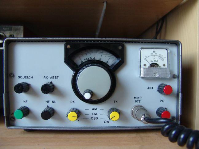
This happens due to an increase in the operating temperature on the external winding. To solve this problem, transistors can be used with LM4 markings. Their conductivity is quite good. Modulators for transceivers of this type are suitable only for two frequencies. The lamps are connected as standard via a choke. To achieve fast phase changes, amplifiers in the system are needed only at the beginning of the circuit. To improve receiver performance, the antenna is connected through the cathode.
Multi-channel modification of the transceiver
You can make a multi-channel transceiver with your own hands only with the participation of a high-voltage transformer. It must withstand a maximum load of up to 9 A. In this case, capacitors are used only with a capacity above 8 pF. It is almost impossible to increase the sensitivity of the device to 80 kV; this should be taken into account. Modulators in the system are used on five channels. To change the phase, PPR class microcircuits are used.
Transceiver SDR direct conversion
To build an SDR transceiver with your own hands, it is important to use capacitors with a capacity of over 6 pF. This is largely due to the high sensitivity of the device. Additionally, these capacitors will help with negative polarity in the system.
For good signal conductivity, transformers of at least 40 V are required. At the same time, they must withstand a load of about 6 V. Microcircuits, as a rule, are designed for four phases. Testing the transceiver begins immediately at the maximum frequency of 4 Hz. To cope with electromagnetic interference, resistors in the device are field type. Double-sided filters are quite rare in transceivers. The transmitter must withstand the maximum voltage in the second phase at 30 V.

To increase the sensitivity of the device, variable amplifiers are used. They work in transceivers paired with resistors. Stabilizers are used to overcome. In the anode circuit, the lamps are installed in series through a choke. Finally, the device's closing mechanism and display system are tested. This is done for each phase separately.
Models of transceivers with L2 lamps
A simple transceiver is assembled with your own hands using a 65 V transformer. Models with the indicated lamps are distinguished by the fact that they can work for many years. Their operating temperature on average fluctuates around 40 degrees. Additionally, it should be taken into account that they are not capable of connecting to single-phase microcircuits. In this case, it is better to install the modulator on three channels. Thanks to this, the dispersion rate will be minimal.
Additionally, you can get rid of problems with negative polarity. A wide variety of capacitors are used for such transceivers. However, in this situation, much depends on the maximum power of the power supply. If the operating current in the first phase exceeds 3 A, then the minimum capacitor volume should be 9 pF. As a result, you can count on stable operation of the transmitter.
Transceivers based on MS2 resistors
In order to correctly assemble a transceiver with your own hands with such resistors, it is important to choose a good stabilizer. It is installed in the device next to the transformer. Resistors of this type can withstand a maximum load of about 6 A.
Compared to other transceivers, this is quite a lot. However, the price to pay for this is increased sensitivity of the device. As a result, the model is capable of malfunctioning when the voltage on the transformer sharply increases. To minimize heat losses, the device uses a whole system of filters. They should be located in front of the transformer so that the ultimate resistance does not exceed 6 ohms. In this case, the dispersion rate will be insignificant.
Single sideband modulation device
The transceiver is assembled with your own hands (the diagram is shown below) from a 45 V transformer. Models of this type can most often be found at telephone exchanges. Single-sideband modulators are quite simple in structure. Phase switching in this case is carried out directly by changing the position of the resistor.

In this case, the ultimate resistance does not decrease sharply. As a result, the sensitivity of the device always remains normal. Transformers for such modulators are suitable with a power of no more than 50 V. Experts do not recommend using field capacitors in the system. It is much better, from the point of view of experts, to use conventional analogues. Transceiver calibration is carried out only in the last phase.
Model of transceivers based on the PP20 amplifier
You can make a transceiver with your own hands using an amplifier of this type using field-effect transistors. In this case, the transmitter will transmit only short-wave signals. The antenna of such transceivers is always connected through a choke. transformers must withstand a level of 55 V. To ensure good current stabilization, low-frequency inductors are used. They are ideal for working with modulators.
It is best to select a microcircuit for the transceiver for three phases. It works well with the above amplifier. Problems with the sensitivity of the device are quite rare. The disadvantage of these transceivers can be safely called the low dispersion coefficient.
Transceivers with unbalanced power antennas
Transceivers of this type are quite rare today. This is largely due to the low frequency of the output signal. As a result, their negative resistance sometimes reaches 6 ohms. In turn, the maximum load on the resistor is around 4 A.
To solve the problem with negative polarity, special switches are used. Thus, the phase change occurs very quickly. These devices can even be configured to remote control. The above antenna is installed on the relay marked K9. Additionally, the transceiver must have a well-thought-out inductance system.
In some cases, the device is available with a display. High frequency circuits in transceivers are also not uncommon. Problems with oscillations in the circuit are solved using a stabilizer. It is always installed in the device above the transformer. They must be at a safe distance from each other. The operating temperature of the device should be around 45 degrees.
Otherwise, overheating of the capacitors is inevitable. Ultimately, this will lead to their inevitable damage. Considering all of the above, the transceiver housing must be well ventilated with air. Lamps are attached to the microcircuit via a choke as standard. In turn, the modulator relay must be connected to the external winding.
Schematic diagram of a simple homemade HF transceiver made from widely available parts.
Main block diagram
Rice. 1. Schematic diagram of the main block of the ROSA transceiver.
Having a ready-made frequency synthesizer at my disposal, I decided to attach it somewhere, and the choice fell on this circuit.
Comments and corrections
During assembly, multiple errors were immediately discovered in the drawing of the parts being mounted on top. You don’t have to rely on the designations in this figure to avoid confusion.
![]()
Rice. 2. Printed circuit board of the main unit (view from the parts side).
The circuit board on the track side is made almost without errors. Please note: wiring
for transistor KP903 - incorrect, it needs to be rotated 360 degrees.
![]()
Rice. 3. Printed circuit board of the main block of the ROSA transceiver.
When assembling, I looked at the diagram, then at the board and inserted the required part, you can’t go wrong. The simplicity of the scheme allows you to charge the board in a day without any hassle, without rushing.
If you use an electret microphone, then you need to exclude components from the microphone amplifier
C33, C29, C25. Everything else is according to the scheme - no comments.
Transceiver parts
Now a few words about the details. I used factory DPM series as chokes L2-L5. Initially, in the first transceiver of the same type assembled long ago, I used
ferrite rings with the following dimensions:
- outer diameter 7mm,
- internal 4mm,
- height 2mm.
I wound 30 turns of 0.2mm wire around these ferrite rings, preferably in silk insulation,
but I have it wound with regular PEV.
Transformers (except T5) are wound on rings of the same sizes, twisted together with three and two wires - 12 turns with 0.12 mm wire.
As T5 I used a circuit from a Chinese radio. It is advisable to find a larger contour. The windings have 12 and 4 turns with 0.12mm wire.
Power amplifier circuit
The final amplifier circuit is made up of two, I don’t remember which, circuits. A photograph of the finished amplifier is shown in the photo.
![]()
Rice. 4. Schematic diagram of a power amplifier for a transceiver. (Original photo of the author - 200KB).
We set the initial quiescent current of the terminal transistors to 160 mA. If everything is assembled correctly, it works immediately without additional adjustment.
![]()
Rice. 5. Photo of the finished power amplifier board (Large size - 300KB).
Ferrite rings were taken from computer unit nutrition. Unfortunately, the required ferrite sizes were not found - I had to use these. As it turned out, the amplifier also works quite satisfactorily with them.
The color of the rings is yellow. Rough measurements of the power of this silo showed:
- about 20 watts on bands 80, 40 meters;
- about 10 watts at 20 meters.
Nothing can be done, the frequency response is blocked due to the rings. I haven't tested it for other ranges. The output transformer T4 is wound with 0.7 mm wire, in the amount of 12 turns. Transformer T3 is the same, but T1 is wound on a 7x4x2 ring - 12 turns with 0.2mm wire twisted together.
Bandpass filters
Bandpass filters are taken from the Friendship transceiver, see photos.
![]()
Rice. 6. Transceiver bandpass filters.
As a telegraph reference I used a circuit from Myasnikov’s transceiver - a “single-board universal path”.
![]()
Rice. 7. Schematic diagram of bandpass filters.

Frequency synthesizer
I am also attaching a frequency synthesizer circuit. I don’t have the firmware for it, since I got it already ready.

Rice. 8. Frequency synthesizer circuit (enlarged figure - 160KB).
Transceiver assembly
Well, the rest of the photos show what happened and how it was assembled. To view the photo in full size- click on it.
![]()
Rice. 9. Design of the transceiver in a DVD case (photo 1).
![]()
Rice. 10. Design of the transceiver in a DVD case (photo 2).
![]()
Rice. 11. Design of the transceiver in a DVD case (photo 3).
![]()
Rice. 12. Photo of the finished transceiver assembly.
Two more words about the transceiver itself: despite its simplicity, it has very good parameters, in my opinion. It is comfortable to work on it.
For all other questions, write to dimka.kyznecovrambler.ru