Now smartphones can process a mountain of information if desired. Their processor power is enough to solve absolutely any problem. At the same time, modern chipsets consume a minimal amount of electricity, for which we should thank the improved technical process. Our rating of smartphone processors will tell you about the most powerful and interesting models. Devices based on them can be blamed for anything, but certainly not for lack of power!
Good to know!
Samsung Exynos 9820

- Year of issue: 2019
- Technical process: 8 nm
- Architecture: 2*Custom + 2*Cortex A75+ 4*Cortex A55
- Video accelerator: Mali-G76 MP12
Geekbench result: 4382/9570 points
An interesting fact was the appearance of the Samsung chipset in third place powerful processors. Previously, the company's solutions in synthetic tests were inferior not only to Qualcomm, but also to Huawei, but in this case the Koreans' numbers were higher.
The new product is built on an 8-nanometer process technology, the cores are divided into 3 groups - two proprietary fourth-generation cores, two productive Cortex A75 and four energy-efficient Cortex A55. Like other manufacturers, the company has focused on improving the performance of neural networks, the security of user data, as well as improving the performance of the camera and supporting a large number of sensors. So the new product can work with 5 cameras including infrared for face scanning and a resolution of no more than 22 megapixels or two front cameras of 16 megapixels each. In addition, the chipset supports 4K displays, shooting in 8K at 30 fps, 4K up to 120 fps.
Advantages:
- Instantly configure camera settings for working with AR and VR.
- Supports shooting in 8K.
- Work with 5 cameras.
- Economical battery consumption.
- Improved encoding of users' personal data.
- 4K video processing up to 150 fps.
- Support for 4K displays.
- Works with UFS 2.1/3.0 SSDs.
Flaws:
- 8 nm process technology – even with the most ideal optimization, these chipsets cannot compete with 7 nm models in energy efficiency.
- Of the 8 cores, only the first two can be called new; the remaining 6 cores were migrated from previous processors without any changes, that is, the new product can hardly be fully considered as such - rather, it is an improved old processor.
Samsung S10, S10+, S10e
Huawei KIRIN 980

- Year of issue: 2018
- Technical process: 7 nm
- Architecture: 2*Cortex-A76 + 2*Cortex A76 + 4*Cortex A55
- Video accelerator: Mali-G76 MP10
Geekbench result: 3390/10318 points
The new processor from Huawei was technically the first created using the 7 nm process technology, however, having presented it to the world, the company was late with the release, giving the laurels to Apple. The cores are divided into three groups - two high-performance, two energy-efficient and four medium-performance. To ensure that exactly the cores needed are used in a particular task, the company has implemented Flex-Scheduling technology, thanks to which performance has increased by 37% compared to last year’s Kirin 970. Not without a new graphics accelerator, which is not only more powerful, but also automatically increases the clock speed in games.
Just like Huawei's competitors have improved the machine unit, it is 120% faster than its predecessor. In this case, these are not just words. Every year, all manufacturers focus on cameras and the fact that thanks to the work of AI, the pictures really turn out better in any conditions is difficult to dispute. This is best seen from Huawei. Already with last year's Kirin 970, the company achieved first place in the most prestigious camera rating from DxOMark. With the new processor, we can expect to surpass the previous level. A lot has been written about the photographic capabilities of the chipset, or more precisely its neural unit. To simplify, Huawei does the following - it does not chase top performance in tests, but it makes really excellent chipsets for photos and videos, and again there will be no difficulties with launching games or any other tasks. In many cases, this is what is required by users who look at real possibilities, not numbers.
Advantages:
- The best processor for photos and videos.
- Two neural network modules.
- Supports high-speed LPDDR4X RAM up to 16GB.
- Flex-Scheduling is a technology for choosing the “right” cores for specific tasks, which results in excellent energy efficiency and fast loading any applications.
- HDR10+ support.
- Support for the new standard - Wi-Fi 802.11ay.
- Work with 48 MP cameras or dual 22 MP modules.
- 4K recording at 60 fps.
Flaws:
- The graphics coprocessor is weaker than its competitors - this is not a minus for users, since there is GPU Turbo technology for automatic overclocking, which compensates for the difference.
- The company used “old” cores and improved them, that is, in fact, this is an updated processor, and not a fundamentally new development.
- No 5G support.
Most popular smartphones: View 20, Huawei P30, Huawei Mate 20
Mediatek Helio P90
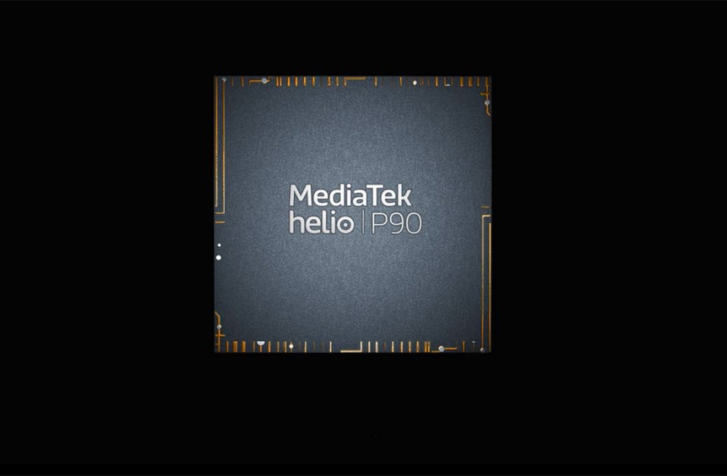
- Year of issue: 2018
- Technical process: 12 nm
- Architecture: 2* Cortex-A75 + 6*Cortex A55
- Video accelerator: PowerVR GM 9446
Geekbench result: 2025/6831 points
MediaTek has long been associated among users with processors for budget and occasionally mid-price smartphones. The company is struggling to create a competitive flagship-level model, but is not doing it very well. So MediaTek did not make it into the top 10 most productive chipsets, but took 11th place with the Helio P90 released in 2019. The model has an eight-core structure, which, although it is divided into two and six cores, is in fact all of them high-performance. Not surprisingly, the P90 was able to outperform the Snapdragon 710 described below, which has exactly the same cores, but with six cores focusing on energy efficiency.
In general, the new product from MediaTek is quite interesting - it supports the fastest RAM and UFS 2.1 solid-state drives, and like its competitors, it can work with a single 48 MP camera or a dual-module solution of 24 and 16 MP. Interesting feature is support for displays with a resolution of 2520*1080 and an aspect ratio of 21:9. The chipset has three image processing units and updated AI with support for AI Fusion function is responsible for distributing tasks among all units - this increases data processing speed. One of the features of this technology is that the screen adapts in real time to the selected application - in particular, when making a video call and switching from full-screen video mode to preview, users will not notice any delays.
Advantages:
- Eight powerful cores for maximum performance.
- Updated AI block for working with photos.
- Supports high-speed LPDDRX memory up to 8 GB.
- Supports modern cameras up to 48 MP.
- Shooting slow-motion video with fps 480 in HD format.
Flaws:
- Not the best energy efficiency.
- No 4K shooting.
- Old generation graphics coprocessor.
The most popular smartphones: BV9800
Qualcomm Snapdragon 710

- Year of issue: 2018
- Technical process: 10 nm
- Architecture: 2* Cortex-A75 + 6*Cortex A55
- Video accelerator: Adreno 616
Geekbench result: 1897 / 5909 points
A mid-level processor that took 12th place in the ranking of the most powerful chipsets. The model became the first in the 700 series. Before this, Qualcomm had a clear division: the 800 series is a flagship level with maximum capabilities, the 600 series is a mid-level with cut-down GPU and CPU cores, and the 400 series is a budget line with a minimum of capabilities. The 700 series processors and in particular the Snapdragon 710 are all the latest chips from the main line and at the same time a fairly affordable price.
The new product runs on two high-performance cores and six energy-efficient ones. Taking into account the new graphics system, the model shows excellent performance in games and at the same time low energy consumption. In addition, it can process photos with high quality - it reduces noise, supports two dual cameras up to 16 MP, and 4K video. The company did not forget about AI, in this case the manufacturer did not waste time on trifles and installed Hexagon 685 machine cores, that is, the same as in 2018 - Snapdragon 845. The result is a fairly inexpensive chipset, which, if inferior to flagships, is only slightly . For those looking for a mid-price smartphone with excellent performance, energy efficiency and photo processing, the Snapdragon 710 will be a real find.
Advantages:
- Affordable price.
- Supports two cameras up to 16 MP.
- Low power consumption.
- Powerful AI for photo creation.
- Supports 4K at 30 fps and HDR.
- Working with biometric sensors.
- Quick Charge 4+ support.
Flaws:
The most popular smartphones:Samsung Galaxy A8s, 16, Xiaomi Mi8 SE
Conclusion
It is worth noting that our rating did not include the Snapdragon 845 and 660, Kirin 970, Apple A11, Exynos 8895, Helio X30 chipsets due to the fact that they were all released at the end of 2017 or the beginning of 2018. Despite their relevance, many readers are familiar with them, and there are a huge number of smartphones based on them. For this reason, we chose powerful new products, which does not entail recommendations for purchasing devices based solely on them. But if you want a smartphone with the latest and most powerful chipset, then the models presented above are the best of their kind.
Removed from selection
Samsung Exynos 8 Octa 8890

- Year of issue: 2016
- Technical process: 14 nm
- Architecture: Samsung Exynos M1+ARM Cortex-A53 (ARMv8-A)
- Video accelerator: Mali-T880, 12 cores, 650 MHz
Geekbench result: 5940 points
If not the best processor for a smartphone, then at least one of those worthy of this title. It’s not for nothing that all variations of the South Korean Galaxy S7 are equipped with it. Is it possible to blame this flagship for lack of power? The chipset can easily handle 4K video at 60 fps. It consists of eight cores. The maximum frequency is 2290 MHz. But it rarely comes to raising it to such a level, since lower frequencies are quite enough to solve most problems.
Unfortunately, the processor also has certain problems. It just so happens that South Korean chipsets are not equipped with the best video accelerator (GPU). Here too, the Mali-T880, despite its 12 cores, performs strictly to the “good” rating, but nothing more. This is proven by tests in GFXBench, where in terms of graphics, the Samsung Exynos 8 Octa 8890 is ahead of some other chipsets reviewed today.
Advantages
- Supports video in 2160p resolution at 60 frames/s;
- Not very hot;
- Low energy consumption;
- High scores in benchmarks.
Flaws
- The memory test does not show the best results;
- The graphics accelerator could perform better.
The most popular smartphones: Samsung Galaxy S7, Samsung Galaxy S7 Edge, Samsung Galaxy Golden 4
Qualcomm Snapdragon 820 MSM8996

- Year of issue: 2015
- Technical process: 14 nm FinFET
- Architecture: Qualcomm Kryo
- Video accelerator: Adreno 530, 624 MHz
Geekbench result: 4890 points
Qualcomm does not have its own production facilities. However, it has many patents at its disposal. And with them, developing a processor close to ideal is not difficult, after which all that remains is to place an order for production from other companies. I am pleased with both the computing power and the capabilities in terms of graphics processing. Many flagships released in 2016 were equipped with this chipset. And none of their customers complained about the graphics in mobile games!
The chip consists of only four cores. However, this did not stop it from scoring record scores in benchmarks - not least thanks to the graphics accelerator. The maximum frequency of this processor is 2150 MHz. At the hardware level, the chipset supports HDMI 2.0, USB 3.0, and Bluetooth 4.1. In short, the processor could easily cope even with the tasks assigned to a laptop! It also features camera support with a resolution of up to 28 megapixels - which is why the company chose this processor, in flagship smartphones which contains just such a sensor.
Advantages
- Very high resolution camera support;
- Capable of processing Full HD video at up to 240 frames/s;
- Supports 10-bit 4K video;
- Windows devices use DirectX 11.2;
- Very high clock speed;
- Not very high energy consumption;
- High scores in benchmarks;
- The memory test leads to high results;
- Excellent performance in games.
Flaws
- Sometimes it gets quite hot.
The most popular smartphones: Moto Z Force, Elite X3, ZenFone 3, 10, Samsung Galaxy S7, Samsung Galaxy S7 Edge, Sony Xperia X Performance, Sony Xperia XR, Xiaomi Mi5 Pro, Z11
HiSilicon Kirin 95

- Year of manufacture: 2016
- Technical process: 16 nm
- Architecture:
- Video accelerator: Mali-T880, 4 cores
Geekbench result: 6000 points
This chipset is manufactured using a 16-nanometer process technology, which indicates its decent energy efficiency. The maximum frequency here is increased to 2.5 GHz. The creators had to take this step because of the Mali-T880 graphics accelerator, which does not cope with its task in the best way.
The Chinese chipset consists of eight cores, four of which can be called auxiliary. Paired with a GPU, it is capable of playing 4K video at 60 fps. But the processor can only playback - independently create video recordings - in 1080p resolution. And this despite the fact that the chip even supports dual cameras, the total resolution of which is 42 megapixels. He is also able to recognize Bluetooth modules 4.2 and USB 3.0.
Advantages
- Support for many modern wireless technologies;
- Almost record clock speed;
- There are no big problems with overheating;
- Can decode 4K video at 60fps;
- Supports dual high definition cameras.
Flaws
- The graphics accelerator shows poor results.
The most popular smartphones: Huawei P9, Huawei P9 Plus, Huawei Honor V8, Huawei Honor Note 8.
HiSilicon Kirin 950
- Year of issue: 2015
- Technical process: 16 nm
- Architecture: 4x ARM Cortex-A72 + 4x ARM Cortex-A53
- Video accelerator: Mali-T880, 4 cores, 900 MHz
Geekbench result: 5950 points
In 2015-2016, this processor was used by many Huawei smartphones. The chipset consists of eight cores, the power of four of them can reach 2300 MHz. It would seem that the result is quite good. But not everything is so simple. The weak point of the chip is the graphics accelerator. The first version of Mali-T880 is used here. It copes well with video decoding - in theory, you can even run 4K video at 60 frames/s. But in games this GPU performs disgustingly, especially by flagship standards.
However, you can’t find fault with the computing power of this chipset, which is why it made it into our top processors. The product supports Bluetooth 4.2 and USB 3.0 standards, although the Chinese giant has not really produced smartphones with such high-speed interfaces, preferring to save. Also, in theory, the processor copes with the data stream from, which has a total resolution of 42 megapixels.
Advantages
- Supports USB 3.0 and Bluetooth 4.2;
- High computing power;
- Support for modern memory formats;
- Not very expensive to produce;
- Decodes video into high resolution;
- Capable of handling a dual 42-megapixel camera.
Flaws
- The graphics accelerator could be much better;
- Cannot provide the camera with 4K video recording.
The most popular smartphones: Huawei Honor 8, Huawei Honor Note 8, Huawei Mate 8, Huawei Honor V8.
Apple A9X APL1021

- Year of issue: 2015
- Technical process: 16 nm
- Architecture: Apple Twister 64-bit ARMv8-compatible
- Video accelerator: PowerVR Series 7X, 12 cores
Geekbench result : 5400 points
Why are game developers primarily targeting smartphones and Apple tablets? Is it really only their owners who can afford to buy a toy? No, everything is much simpler. This is the technique that games work best on. The Apple A9X APL1021 processor is equipped with an almost ideal graphics accelerator, which can solve absolutely any problem! If Apple wanted, it could even implement a 4K video recording feature at 60 frames per second!
As for computing power, everything is fine here, although the processor still does not score record scores in benchmarks. It would seem that only two cores are used here. But for a solution daily tasks this is quite enough. Not least because of the better optimized operating system.
Advantages
- High power of two cores;
- Excellent 12-core graphics accelerator;
- Full support for 4K video at 60 fps;
- Support from many modern technologies;
- Recognizes modern memory formats.
Flaws
Apple iPad Pro
MediaTek MT6797 Helio X25

- Year of issue: 2016
- Technical process: 20 nm
- Architecture: 2x ARM Cortex-A72 + 4x ARM Coptex-A53 + 4x ARM Coptex-A53
- Video accelerator: Mali-T880MP4, 4 cores, 850 MHz
Geekbench result: 4920 points
A processor with a fairly complex structure. It consists of ten nuclei belonging to two varieties. The two cores are the most powerful - they belong to the Cortex-A72 type, and their clock speed can reach 2500 MHz. The remaining computing cores belong to the Cortex-A53 type. Moreover, half of them are overclocked to a frequency of 2000 MHz, while the rest are limited to 1550 MHz.
All this allows the processor to score a lot of points in benchmarks. And the result would have been even higher if not for the graphics accelerator. This element here is seriously limited in its capabilities. Yes, it supports full work with 4K video, including its creation, but only at 30 fps. And in games the GPU copes with its task even worse. As for other characteristics, we should highlight support for 32-megapixel cameras and the Bluetooth 4.1 standard. The maximum display resolution of a smartphone with such a chipset can reach 2560 x 1600 pixels.
Advantages
- Support for 32 MP camera;
- Very high computing power;
- Relatively low energy consumption;
- Although limited, there is support for 4K video;
- Low cost chipset.
Flaws
- The GPU performs poorly in games;
- No Bluetooth 4.2 support.
The most popular smartphones: Meizu Pro 6, K6000 Premium, Xiaomi Redmi Pro, Speed 8, Apollo.
Qualcomm Snapdragon 625 MSM8953

- Year of issue: 2016
- Technical process: 14 nm
- Architecture: ARM Cortex-A53 (ARMv8)
- Video accelerator: Adreno 506
Geekbench result: 4900 points
One of Qualcomm's most popular creations. It is endowed with a huge number of smartphones from the mid-budget and even top segments. The manufacturer did not bother with the architecture, giving the chipset eight identical cores. The maximum clock frequency is 2000 MHz, which is quite enough for the average user.
The graphics accelerator here is optimized for processing video content. Theoretically, a smartphone built on the basis of this processor is capable of playing and recording 4K video at 60 frames per second. But in games some problems begin. Although their presence is surprising, because the GPU even has support for DirectX 12, which is activated on devices with Windows on board. The chipset also supports a dual camera, the total resolution of which does not exceed 24 megapixels. The only thing missing here is USB 3.0 support. However, smartphone creators do not like to integrate such high-speed connectors into their creations.
Advantages
- Dual camera supported;
- Well implemented technology fast charging;
- High power of all eight cores;
- Full support for 4K video content at 60 fps;
- Relatively low cost.
Flaws
- Camera resolution cannot exceed 24 megapixels;
- No Bluetooth 4.2 support;
- Display resolution cannot exceed 1920 x 1200 pixels;
- In games, the chipset does not perform well.
The most popular smartphones: Huawei G9 Plus, ASUS ZenFone 3, Fujitsu Easy, Huawei Maimang 5, Vibe P2, Motorola Moto Z Play, Samsung Galaxy C7.
Qualcomm Snapdragon 620 APQ8076

- Year of issue: 2016
- Technical process: 28 nm
- Architecture: 4x ARM Cortex-A72 + 4x ARM Cortex-A53
- Video accelerator: Adreno 510
Geekbench result: 4886 points
This chipset is also known as Snapdragon 652. It is one of the latest processors, which is still produced on a 28nm process. The creators are not at all embarrassed by the relatively large size of the chip, since it is built mainly into tablets.
The processor consists of eight computing cores. The clock frequency of four of them can reach 1800 MHz. This is quite enough for the tablet to solve basic tasks without any hesitation. The chipset also includes the Adreno 510 graphics accelerator. There are no special complaints about it, because no one will expect excellent graphics performance from the tablet. It should be noted that theoretically the chip supports video processing in 2160p resolution at 30 frames/s. It also boasts support for Bluetooth 4.1 and proprietary Quick Charge 3.0 fast charging technology.
Advantages
- Supports devices with high screen resolutions;
- Great computing power;
- Albeit limited, but still support for 4K video;
- Built-in fast charging technology.
Flaws
- No Bluetooth 4.2 support;
- Still not the best graphics accelerator.
Most popular devices: Samsung Galaxy Tab S2 Plus 8.0, Samsung Galaxy Tab S2 Plus 9.7.
MediaTek MT6797M Helio X20

- Year of issue: 2016
- Technical process: 20 nm
- Architecture: 2x ARM Cortex-A72 + 4x ARM Cortex-A53 + 4x ARM Cortex-A53
- Video accelerator: Mali-T880MP4, 4 cores, 780 MHz
Geekbench result: 5130 points
Many mobile processors have four or even eight cores. In the case of the MediaTek MT6797M Helio X20, their number has been increased to ten. As a result, the performance of the chipset is very high. Especially in applications that do not require serious graphics processing. It should be noted that only two computing cores are particularly powerful here - their clock frequency reaches 2300 MHz. The remaining nuclei are divided into two groups. One can please you with a frequency of 1850 MHz, while the other has this parameter fixed at 1400 MHz. But the result in any case is very good, which is confirmed by synthetic tests, and by the smartphones themselves - the interface on them does not slow down at all thanks to the chipset.
As for the graphics accelerator, everything is much worse here. Theoretically, it copes with viewing and recording 4K video at 30 frames per second. But in games you immediately feel a lack of power. Modern games will run on a smartphone with such a processor, but with simplified graphics. Especially if the device has a screen with Full HD resolution or higher. It should also be noted that the processor supports almost any mobile cameras- as long as the module resolution does not exceed 32 megapixels.
- Year of issue: 2015
- Technical process: 28 nm
- Architecture: ARM Cortex-A72 + ARM Cortex-A53 (ARMv8)
- Video accelerator: Adreno 510
Geekbench result: 4610 points
There are two versions Qualcomm processor Snapdragon 620, also known as Snapdragon 652. The first is MSM8976, this chipset was released in 2015. A year later, a slightly more improved version was released - APQ8076, which some received. The products are practically no different from each other. They have eight cores, half of which are capable of increasing the frequency to 1800 MHz. Both processors are equipped with a far from ideal Adreno 510 graphics accelerator.
Qualcomm's creation is capable of supporting smartphones whose display has a resolution of no higher than 2560 x 1600 pixels. As for the camera, it is possible to process data coming from a dual module, the total resolution of which does not exceed 21 megapixels. Everything is fine with the module and its capabilities for processing data coming from dual-channel LPDDR3 memory.
Advantages
- High performance;
- View 4K video at 30 fps;
- Theoretical possibility of recording video in 1080p and 120 frames/s;
- Not very high cost;
- Dual camera support;
- Screen resolution can reach 2560 x 1600 pixels.
Flaws
- Bluetooth 4.2 is not supported;
- The maximum camera resolution cannot be very high.
The most popular smartphones: X6S A, Vivo X7, Vivo X7 Plus, LeEco Le2, G5 SE, R9 Plus, Samsung Galaxy A9 Pro (2016), ZTE Nubia Z11 Max, Xiaomi Mi Max
Sergey Pakhomov
Sales of laptops have long surpassed sales of desktop PCs, and today most home users rely on laptops. IN retail network A huge number of different laptop models are offered on both Intel and AMD platforms. On the one hand, such abundance pleases the eye, but on the other, the problem of choice arises. As you know, the performance of a computer is largely determined by the processor installed in it, but understanding modern families and symbols of processors is not so easy. And if with the designations of mobile processors Intel everything is more or less clear, but AMD is in complete confusion with this. Actually, it was precisely this circumstance that prompted us to compile a kind of guide to mobile processors from AMD.
The range of AMD processors for laptops is more than diverse (see table). However, if we talk about modern processors, which it makes sense to focus on, then we can limit ourselves to considering only 45-nm processors of the Phenom II, Athlon II, Turion II, V-series, Sempron families with the following core code names: Champlain, Geneva and Caspian.
Processors codenamed Champlain were announced by the company quite recently - in May 2010, while 45 nm processors codenamed Caspian were announced in September 2009.
The AMD family of mobile processors includes both quad-core and triple-, dual- and single-core models.
Each processor core has a 128 KB Level 1 (L1) cache, which is divided into a dual-channel 64 KB data cache and a dual-channel 64 KB instruction cache. In addition, each processor core has a dedicated L2 cache of 512 KB or 1 MB.
But AMD mobile processors do not have third-level cache memory (L3) (unlike their desktop counterparts).
All AMD mobile processors feature AMD 64 technology (64-bit computing support). In addition, all AMD processors are equipped with MMX, SSE, SSE2, SSE3 and Extended 3DNow! instruction sets, Cool'n'Quiet power saving technologies, NX Bit virus protection and AMD Virtualization technology.
So, let's look at the families of modern AMD mobile processors in more detail. And we will begin, naturally, by considering the AMD Phenom II family of quad-core processors.
AMD's mobile quad-core processor family is the 900 series of Phenom II processors.
All Phenom II 900 series processors have a 2 MB L2 cache (512 KB per processor core) and an integrated DDR3 memory controller. Additionally, all of these processors use 128-bit FPUs. The differences between the quad-core Phenom II 900 series processors include clock speed, power consumption, and supported memory. For its processors, AMD indicates another rather strange and, in our opinion, completely illogical characteristic - Maximum processor-to-system bandwidth (MAX CPU BW). We are talking about the total bandwidth of all buses between the processor and the system, or rather, the total bandwidth HyperTransport tires(HT) and memory buses. If, for example, the processor works with DDR3-1333 memory, then throughput memory bus is 21.2 GB/s (in dual-channel mode). Further, if the HyperTransport (HT) bus throughput is 3600 GT/s, which corresponds to a throughput of 14.4 GB/s, then the total throughput of the HyperTransport bus and the memory bus will be 35.7 GB/s. Of course, it would be more logical to indicate in the processor specification the maximum memory frequency that the processor supports, but... it is what it is. Fortunately, knowledge of the HyperTransport bus bandwidth and such a parameter as MAX CPU BW allows you to unambiguously determine the maximum memory frequency supported by the processor.
So, let's return to the family of quad-core Phenom II 900 series processors. This family is headed by the Phenom II X920 Black Edition (BE) with unlocked multiplier. This processor has the highest clock speed (2.3 GHz) in the AMD family of quad-core mobile processors and is the hottest - its power consumption is 45 W. The HyperTransport bus bandwidth is 3600 GT/s, and the MAX CPU BW parameter value is 35.7 GB/s. As you can easily calculate, this means that the built-in DDR3 memory controller supports memory with a maximum frequency of 1333 MHz (in dual-channel operating mode).
Two more models of AMD quad-core mobile processors are the Phenom II N930 and Phenom II P920. The Phenom II N930 has a clock speed of 2 GHz and a power consumption of 35 W, while the Phenom II P920 has a clock speed of 1.6 GHz and a power consumption of 25 W. For both processor models, the HyperTransport bus bandwidth is 3600 GT/s, but the Phenom II N930 processor supports DDR3-1333 memory, and the Phenom II P920 processor only supports DDR3-1066 memory.
AMD's tri-core mobile processor family is the 800 series of Phenom II processors. Today there are only two three-core models of mobile processors: Phenom II N830 and Phenom II P820, both equipped with a 1536 KB L2 cache (512 KB for each processor core) and an integrated DDR3 memory controller. The difference between these models is the clock speed, power consumption and the maximum frequency of supported DDR3 memory. Thus, the Phenom II N830 processor operates at a clock frequency of 2.1 GHz with a power consumption of 35 W, and the maximum frequency of DDR3 memory supported by the processor is 1333 MHz. The Phenom II P820 processor operates at a clock speed of 1.8 GHz with a power consumption of 25 W and supports DDR3-1066 memory.
In passing, we note that if the letter “P” is present in the marking of AMD processors, this means that the processor’s power consumption is 25 W. The presence of the letter “N” indicates a processor power consumption of 35 W, and the letter “X” indicates 45 W.
The Phenom II family of dual-core processors is the 600 series. This series today includes two models: Phenom II X620 BE and Phenom II N620. Both of them have a 2 MB L2 cache (1 MB per core) and 3600 GT/s HT bus bandwidth. Moreover, both processor models support DDR3-1333 memory (MAX CPU BW is 35.7 GB/s). The difference between the processors is that the Phenom II X620 BE model has a power consumption of 45 W and a clock speed of 3.1 GHz. In addition, this processor has an unlocked multiplier. The Phenom II N620 processor with a power consumption of 35 W has a clock speed of 2.8 GHz.
Concluding the review of mobile processors of the Phenom II family, we note once again that it includes four, triple and dual-core processors with a 128-bit FPU, the power consumption of which can be 45, 35 or 25 W. All of these processors have HT 3600 GT/s bus bandwidth and support DDR3 memory with a maximum frequency of 1333 or 1066 MHz. The size of the L2 cache depends on the number of processor cores and per one processor core is 512 KB (for four and three-core models) or 1 MB (for dual-core models).
The next family of 45nm mobile processors based on the Champlain core is the Turion II family of dual-core processors, which is represented by two models: Turion II N530 and Turion II P520. These processors differ from each other only in clock speed and power consumption. The Turion II N530 has a clock speed of 2.5 GHz and a power consumption of 35 W, while the Turion II P520 has a clock speed of 2.3 GHz and a power consumption of 25 W. In all other respects, the characteristics of these processors are the same. Thus, both models are equipped with 128-bit FPUs, have a 2 MB L2 cache (1 MB per core), and the HT bus bandwidth is 3600 GT/s. In addition, both processor models support DDR3-1066 memory. Note that the dual-core processors of the Turion II 500 series family are practically no different in their characteristics from the dual-core models of the Phenom II 600 series processors. The differences are only in the clock speed and the maximum frequency of supported memory. Actually, it’s not very clear why these two processor models needed to be separated into a separate Turion II family, because they could be classified as part of the Phenom II family of dual-core processors.
The next family of AMD dual-core mobile processors based on the Champlain core is the Athlon II family, which is also represented by two models: Athlon II N330 and Athlon II P320. These processors are really very different from the dual-core Phenom II and Turion II processors. First of all, their L2 cache is reduced to 1 MB (512 KB per core). In addition, these processors have 64-bit FPUs and an HT bus bandwidth of 3200 GT/s. In addition, these processors only support DDR3-1066 memory. The differences between the Athlon II N330 and Athlon II P320 models themselves are in clock speed and power consumption.
Single-core mobile processors based on the Champlain core are represented by the V-Series family, which today includes only one model - the V120 with a clock frequency of 2.2 GHz and a 512 KB L2 cache. This processor is equipped with 64-bit FPUs, and the HT bus bandwidth is 3200 GT/s. In addition, the V120 processor supports DDR3-1066 memory and its power consumption is 25 W. In general, according to its characteristics, the V120 processor is a single-core version of the Athlon II P320 processor.
All of the AMD mobile processors we reviewed are 2010 processors (the company announced them in May) aimed at performance, general purpose, and entry-level laptops. However, AMD's product range also includes processors with reduced power consumption - they are aimed at ultra-thin laptops and netbooks. These dual-core and single-core 45nm processors, also announced in May, are codenamed Geneva and include the Turion II Neo, Athlon II Neo and V-Series
Dual-core processors of the Turion II Neo series (Turion II Neo K665, Turion II Neo K625) have a power consumption of 15 W, dual-core and single-core processors of the Athlon II Neo series (Athlon II Neo K325, Athlon II Neo K125) have a power consumption of 12 W, but the power consumption of a single-core The V105 processor is only 9 Watts.
The Turion II Neo series dual-core processors feature 128-bit FPUs and 2 MB L2 cache (1 MB per core). The HT bus capacity is 3200 GT/s.
Athlon II Neo series processors have 64-bit FPUs and 1 MB L2 cache per core, and HT bus bandwidth is 2000 GT/s. Well, the single-core V105 processor differs (except for the clock frequency) from the single-core Athlon II Neo K125 processor in that the L2 cache is halved.
Note that all Geneva processors support DDR3-1066 memory in dual-channel mode.
In addition to the Champlain and Geneva mobile processors, AMD's product range also includes other 45 nm mobile processors. We are talking about processors codenamed Caspian, which were announced in September 2009 and are not yet outdated. Caspian mobile processors are represented by the Turion II and Turion II Ultra dual-core processor families, the Athlon II dual-core processor family, and the Sempron single-core processor family.
All dual-core Caspian processors have a power consumption of 35 W, and single-core processors have a power consumption of 25 W. In addition, all Caspian processors only support DDR2-800 memory (in dual-channel operating mode).
The Turion II and Turion II Ultra processor families feature 128-bit FPUs and HT bus bandwidth of 3600 GT/s. The difference between the Turion II Ultra and Turion II family of processors is that the Turion II Ultra processors have a 2 MB L2 cache (1 MB per core), while the Turion II processors have a 1 MB L2 cache (512 KB per core).
Processors of the Athlon II and Sempron families have 64-bit FPUs and 512 KB L2 cache per core. In addition, the HT bus bandwidth for these processors is 3200 GT/s.
When choosing an AMD processor, you are faced with many strange letters and numbers. What do they mean? How to separate an average processor from a weak one? You will learn about this in our material.
Introduction
Processors produced before 2010 will not be considered here, as well as server solutions, chips on the AM1 platform, as well as the AMD Ontario line (on this moment not relevant), so the markings shown in this article may not apply to them.
Here is a video that will help you figure it out, but we recommend that you still read the article, as it is more detailed and will be updated in the future.
Architecture
The market currently offers chips from the 4 latest desktop architectures, and in the second half of 2016 it is planned to introduce to the world a new Zen architecture with a large jump in performance per clock and reduced to 14 nm, which may help catch up with Intel in the top segment.
Sockets
Current platforms at the beginning of 2016 include FM2, FM2+ and AM3+
Processor lines
E - series
Budget entry-level processors designed for laptops and netbooks.
E1 have 2 cores on board, and E2 - 4.
Belonging to a particular generation is determined by the first digit:
- 7-Carrizo-L
- 6 - Beema
- 2, 3 - Kabini (not taking into account old chips before 2012, which have the same number)
There are quite a few chips in this series, and if there is a need, you can familiarize yourself with the models at.
APU
AMD processors with integrated graphics core (APU) are divided into lines:
- A4 – 2 cores
- A6 – 2 cores
- A8 – 4 cores
- A10 – 4 cores
A12-8800B falls out of this nomenclature, but you can read about it.
Accordingly, from weaker to more powerful, both in graphics and in the processor part. Here's an example:

The first digit indicates the processor cores (generation).
| GENERATION | NUMBER IN THE CHIP NAME |
|---|---|
| Carrizo | 8 |
| Godavari | 7 |
| Kaveri | 7 |
| Richland | 4, 6 |
| Trinity | 4, 5 |
In our case, having the number 7, we get Kaveri kernels.
It is worth noting that the number 4 for the A4 series on Richland architecture means a reduced frequency, which leads to reduced performance.
850 – indicates performance among similar processors in frequency (more is better)
- P – standard power consumption in the case of mobile processors (35 W)
- B – designation of Pro processors
- M – mobile processor (old designation)
- K – unlocked for overclocking
- T – reduced energy consumption(desktop PCs)
Interestingly, there are A-processors labeled with the FX trademark. As a rule, these are the company's most powerful laptop processors. They are also built on APU architecture.
Athlon
Now let's talk about Athlon. Essentially these are the same A-processors, but with a disabled video core for a lower price.
Let's take as an example

- X4 – denotes 4 processor cores
- 8 – is an index of Kaveri cores (7 – Trinity)
We see no point in pointing to earlier models, since even the top-end Athlon X4 860K chip for this socket demonstrates the results of an average chip by modern standards, so we do not advise you to buy these processors in 2016. If at first you are satisfied with it, then when upgrading you will have to change the motherboard, which will cost a pretty penny and will recoup the money saved on this decision.
- 60 – just like in the previous case, indicates the position of the processor in the lineup
- K – has the same meaning
FX
Now let's talk about the fastest AMD processors - the FX series. These chips have great overclocking potential and a very affordable price tag. The main disadvantage stems from the rather outdated architecture and production technology - energy consumption. The TDP - performance ratio is greatly inferior Intel processors, but the price - performance is at a very good level. The nomenclature outlined below is not valid for FX 9xxx - these are the same 8xxx, but with an increased clock frequency. Here is the chip we chose as an example:

The first digit indicates the number of cores, in this case 8.
The second indicates a generation
- 3 – Vishera cores
- 1, 2 – Zambezi cores
The remaining numbers indicate the frequency of the chip within the same family, but we believe that this does not matter. We advise you to take the youngest model in the line, since the older ones are exactly the same, but with factory overclocking. Why overpay for factory overclocking if the “stones” drive so well?
If you have any questions, you can visit the website, you can find some useful information there.
This article did not provide information about older chips, as well as about server solutions due to the outdated technology (technical process, architecture) of the former and the specificity of application and high cost of the latter. We hope that our material helped you understand the range of AMD processors and will help you make your choice.
At a special event before CES 2018, AMD released new mobile processors and announced desktop chips with integrated graphics. And Radeon Technologies Group, a structural division of AMD, announced Vega mobile discrete graphics chips. The company also revealed plans to switch to new technical processes and promising architectures: Radeon Navi graphics and Zen+, Zen 2 and Zen 3 processors.
New processors, chipset and cooling
The first Ryzen desktops with Vega graphics
Two Ryzen desktop models with integrated Vega graphics will go on sale on February 12, 2018. The 2200G is an entry-level Ryzen 3 processor, while the 2400G is a mid-range Ryzen 5 processor. Both models dynamically boost clock speeds by 200 and 300 MHz from base frequencies of 3.5 GHz and 3.6 GHz, respectively. In fact, they replace the ultra-budget models Ryzen 3 1200 and 1400.
The 2200G has only 8 graphics units, while the 2400G has 3 more. The frequency of the 2200G graphics cores reaches 1,100 MHz, and the 2400G is 150 MHz more. Each graphics unit contains 64 shaders.
The cores of both processors have the same code name as mobile processors with integrated graphics - Raven Ridge (literally Raven Mountain, a rock formation in Colorado). But nevertheless, they are connected to the same LGA AMD AM4 socket as all other Ryzen 3, 5 and 7 processors.
Reference: Sometimes AMD calls processors with integrated graphics not CPU (Central Processing Unit, English Central processing unit), and APU (Accelerated Processor Unit, English. Accelerated processing unit, in other words, a processor with a video accelerator).
AMD desktop processors with integrated graphics are marked with a G at the end, after the first letter of the word graphics ( English graphic arts). Mobile processors from both AMD and Intel are marked with the letter U at the end, after the first letter of the words ultrathin ( English ultra-thin) or ultra-low power ( English ultra-low power consumption) respectively.
At the same time, you should not think that if the model numbers of the new Ryzen begin with the number 2, then their core architecture belongs to the second generation of the Zen microarchitecture. This is not true - these processors are still in the first generation.
| Ryzen 3 2200G | Ryzen 5 2400G | |
| Cores | 4 | |
| Streams | 4 | 8 |
| Base frequency | 3.5 GHz | 3.6 GHz |
| Increased frequency | 3.7 GHz | 3.9 GHz |
| Level 2 and 3 cache | 6 MB | 6 MB |
| Graphics blocks | 8 | 11 |
| Maximum graphics frequency | 1 100 MHz | 1 250 MHz |
| CPU socket | AMD AM4 (PGA) | |
| Base Heat Dissipation | 65 W | |
| Variable heat dissipation | 45-65 W | |
| Codename | Raven Ridge | |
| Recommended price* | 5,600 ₽ ($99) | 9,500 ₽ ($99) |
| release date | February 12, 2018 | |
New Ryzen mobiles with Vega graphics
Last year, AMD already brought the first mobile Ryzen to the market under the code name Raven Ridge. The entire Ryzen mobile family is designed for gaming laptops, ultrabooks and tablet-laptop hybrids. But there were only two such models, each in the middle and high-end segments: Ryzen 5 2500U and Ryzen 7 2700U. The junior segment was empty, but the company corrected this right at CES 2018 - two models were added to the mobile family: Ryzen 3 2200U and Ryzen 3 2300U.
AMD Vice President Jim Anderson demonstrates the Ryzen mobile family
The 2200U is the first dual-core Ryzen CPU, while the 2300U is quad-core as standard, but both run four threads. At the same time, the base frequency of the 2200U cores is 2.5 GHz, and the lower 2300U is 2 GHz. But with increasing loads, the frequency of both models will rise to the same level - 3.4 GHz. However, laptop manufacturers can lower the power ceiling, because they also need to calculate energy costs and think through the cooling system. There is also a difference in cache size between the chips: the 2200U has only two cores, and therefore has half the cache of levels 1 and 2.
The 2200U has only 3 graphics units, but the 2300U has twice as many, as well as processor cores. But the difference in graphics frequencies is not so significant: 1,000 MHz versus 1,100 MHz.
| Ryzen 3 2200U | Ryzen 3 2300U | Ryzen 5 2500U | Ryzen 7 2700U | |
| Cores | 2 | 4 | ||
| Streams | 4 | 8 | ||
| Base frequency | 2.5 GHz | 2 GHz | 2.2 GHz | |
| Increased frequency | 3.4 GHz | 3.8 GHz | ||
| Level 1 cache | 192 KB (96 KB per core) | 384 KB (96 KB per core) | ||
| Level 2 cache | 1 MB (512 KB per core) | 2 MB (512 KB per core) | ||
| Level 3 cache | 4 MB (4 MB per complex of cores) | |||
| RAM | Dual channel DDR4-2400 | |||
| Graphics blocks | 3 | 6 | 8 | 10 |
| Maximum graphics frequency | 1,000 MHz | 1 100 MHz | 1 300 MHz | |
| CPU socket | AMD FP5 (BGA) | |||
| Base Heat Dissipation | 15 W | |||
| Variable heat dissipation | 12-25 W | |||
| Codename | Raven Ridge | |||
| release date | January 8, 2018 | October 26, 2018 | ||
The first mobile Ryzen PRO
AMD has planned release for the second quarter of 2018 mobile versions Ryzen PRO, enterprise level processors. The characteristics of the mobile PROs are identical to the consumer versions, with the exception of the Ryzen 3 2200U, which did not receive a PRO implementation at all. The differences between desktop and mobile Ryzen PRO are in additional hardware technologies.
 Ryzen PRO processors are complete copies of regular Ryzen, but with additional features
For example, TSME, on-the-fly hardware encryption of RAM, is used to ensure security (Intel only has software-intensive SME encryption). And for centralized management of a fleet of machines, the open standard DASH (Desktop and mobile Architecture for System Hardware) is available. system devices) - support for its protocols is built into the processor.
Laptops, ultrabooks and hybrid tablet-laptops with Ryzen PRO should primarily be of interest to companies and government agencies that plan to purchase them for employees.
| Ryzen 3 PRO 2300U | Ryzen 5 PRO 2500U | Ryzen 7 PRO 2700U | |
| Cores | 4 | ||
| Streams | 4 | 8 | |
| Base frequency | 2 GHz | 2.2 GHz | |
| Increased frequency | 3.4 GHz | 3.6 GHz | 3.8 GHz |
| Level 1 cache | 384 KB (96 KB per core) | ||
| Level 2 cache | 2 MB (512 KB per core) | ||
| Level 3 cache | 4 MB (4 MB per complex of cores) | ||
| RAM | Dual channel DDR4-2400 | ||
| Graphics blocks | 6 | 8 | 10 |
| Maximum graphics frequency | 1 100 MHz | 1 300 MHz | |
| CPU socket | AMD FP5 (BGA) | ||
| Base Heat Dissipation | 15 W | ||
| Variable heat dissipation | 12-25 W | ||
| Codename | Raven Ridge | ||
| release date | Second quarter 2018 | ||
New AMD 400 series chipsets
The second generation of Ryzen relies on the second generation of system logic: the 300th series of chipsets is replaced by the 400th. The flagship of the series, as expected, was the AMD X470, and later simpler and cheaper sets of circuits, such as the B450, would be released. The new logic has improved everything related to RAM: it has reduced access latency, raised the upper frequency limit, and added headroom for overclocking. Also in the 400 series, USB bandwidth has increased and the processor's power consumption has improved, and at the same time its heat dissipation.

But the processor socket has not changed. The AMD AM4 desktop socket (and its mobile non-removable version AMD FP5) is a special advantage of the company. The second generation has the same connector as the first. It will not change in the third and fifth generations. AMD promised, in principle, not to change AM4 until 2020. And for the 300 series motherboards (X370, B350, A320, X300 and A300) to work with the new Ryzen, you just need to update the BIOS. Moreover, in addition to direct compatibility, there is also reverse compatibility: old processors will work on new boards.
Gigabyte at CES 2018 even showed a prototype of the first motherboard based on the new chipset - the X470 Aorus Gaming 7 WiFi. This and other boards based on X470 and lower chipsets will appear in April 2018, simultaneously with the second generation of Ryzen on the Zen+ architecture.
New cooling system
AMD also introduced the new AMD Wraith Prism cooler. While its predecessor, the Wraith Max, was illuminated in a single color red, the Wraith Prism features motherboard-controlled RGB lighting around the perimeter of the fan. The cooler blades are made of transparent plastic and are also illuminated in millions of colors. Fans of RGB backlighting will appreciate it, and haters can simply turn it off, although in this case the point of buying this model will be negated.
Wraith Prism - a complete copy of Wraith Max, but with backlighting in millions of colors
The remaining characteristics are identical to the Wraith Max: direct contact heat pipes, programmable airflow profiles in overclocking mode and virtually silent operation at 39 dB under standard conditions.
There is no information yet on how much the Wraith Prism will cost, whether it will come bundled with processors, or when it will be available for purchase.
New Ryzen laptops
In addition to mobile processors, AMD is also promoting new laptops based on them. In 2017, HP Envy x360 models were released on mobile Ryzen, Lenovo Ideapad 720S and Acer Swift 3. In the first quarter of 2018, the Acer Nitro 5 series will be added to them, Dell Inspiron 5000 and HP. They all run on last year's mobile Ryzen 7 2700U and Ryzen 5 2500U.

The Acer Nitro family is all about gaming machines. The Nitro 5 line is equipped with 15.6-inch IPS displays with a resolution of 1920 × 1080. And some models will be equipped with a discrete Radeon RX 560 graphics chip with 16 graphics units inside.
The Dell Inspiron 5000 line of laptops offers models with display diagonals of 15.6 and 17 inches, equipped with either hard drives or solid-state drives. Some models in the line will also receive discrete video card Radeon 530 with 6 graphics units. This is a rather strange configuration, because even the integrated graphics of the Ryzen 5 2500U have more graphics units - 8 pieces. But the advantage of a discrete card may be higher clock speeds and separate graphics memory chips (instead of the RAM section).
Price reduction for all Ryzen processors
| Processor (socket) | Cores/Threads | Old price* | New price* |
| Ryzen Threadripper 1950X (TR4) | 16/32 | 56,000 ₽ ($999) | - |
| Ryzen Threadripper 1920X (TR4) | 12/24 | 45,000 ₽ ($799) | - |
| Ryzen Threadripper 1900X (TR4) | 8/16 | 31,000 ₽ ($549) | 25,000 ₽ ($449) |
| Ryzen 7 1800X (AM4) | 8/16 | 28,000 ₽ ($499) | 20,000 ₽ ($349) |
| Ryzen 7 1700X (AM4) | 8/16 | 22,500 ₽ ($399) | 17,500 ₽ ($309) |
| Ryzen 7 1700 (AM4) | 8/16 | 18,500 ₽ ($329) | 17,000 ₽ ($299) |
| Ryzen 5 1600X (AM4) | 6/12 | 14,000 ₽ ($249) | 12,500 ₽ ($219) |
| Ryzen 5 1600 (AM4) | 6/12 | 12,500 ₽ ($219) | 10,500 ₽ ($189) |
| Ryzen 5 1500X (AM4) | 4/8 | 10,500 ₽ ($189) | 9,800 ₽ ($174) |
| Ryzen 5 1400 (AM4) | 4/8 | 9,500 ₽ ($169) | - |
| Ryzen 5 2400G (AM4) | 4/8 | - | 9,500 ₽ ($169) |
| Ryzen 3 2200G (AM4) | 4/4 | - | 5,600 ₽ ($99) |
| Ryzen 3 1300X (AM4) | 4/4 | 7,300 ₽ ($129) | - |
| Ryzen 3 1200 (AM4) | 4/4 | 6,100 ₽ ($109) | - |
Plans until 2020: Navi graphics, Zen 3 processors
2017 was a completely turning point for AMD. After years of troubles, AMD completed development of the Zen core microarchitecture and released the first generation of CPUs: the Ryzen, Ryzen PRO and Ryzen Threadripper family of PC processors, the Ryzen and Ryzen PRO mobile family, and the EPYC server family. In the same year, the Radeon group developed the Vega graphics architecture: Vega 64 and Vega 56 video cards were released on its basis, and by the end of the year, Vega cores were integrated into Ryzen mobile processors.

Dr. Lisa Su, CEO of AMD, assures that the company will release 7 nanometer processors before 2020
The new products not only attracted the interest of fans, but also captured the attention of ordinary consumers and enthusiasts. Intel and NVIDIA had to quickly counter: Intel released six-core Coffee Lake processors, the unplanned second “so” of the Skylake architecture, and NVIDIA expanded the 10th series of video cards based on the Pascal architecture to 12 models.
Rumors about AMD's future plans accumulated throughout 2017. Until now, Lisa Su, CEO of AMD, has only noted that the company plans to exceed the 7-8% annual rate of productivity growth in the electronics industry. Finally, at CES 2018, the company showed a “road map” not just until the end of 2018, but right up to 2020. The basis of these plans is improving chip architectures through the miniaturization of transistors: a progressive transition from the current 14 nanometers to 12 and 7 nanometers.
12 nanometers: second generation Ryzen on Zen+
The Zen+ microarchitecture, the second generation of the Ryzen brand, is based on the 12-nanometer process technology. In fact, the new architecture is a modified Zen. The GlobalFoundries manufacturing standard is being converted from 14nm 14LPP (Low Power Plus) to 12nm 12LP (Low Power). The new 12LP process technology should provide chips with a 10% performance increase.
Reference: The GlobalFoundries network of factories are former production capacity AMD, spun off into a separate company in 2009 and merged with other contract manufacturers. In terms of contract manufacturing market share, GlobalFoundries shares second place with UMC, significantly behind TSMC. Chip developers - AMD, Qualcomm and others - order production both from GlobalFoundries and other factories.
In addition to the new technical process, the Zen+ architecture and chips based on it will receive improved AMD Precision Boost 2 and AMD XFR 2 (Extended Frequency Range 2) technologies. In mobile Ryzen processors you can already find Precision Boost 2 and a special modification of XFR - Mobile Extended Frequency Range (mXFR).
The second generation will see the release of the Ryzen, Ryzen PRO and Ryzen Threadripper family of PC processors, but so far there is no information about updating the generations of the Ryzen and Ryzen PRO mobile family, and the server EPYC. But it is known that some models of Ryzen processors will have two modifications from the very beginning: with graphics integrated into the chip and without it. Entry- and mid-level models Ryzen 3 and Ryzen 5 will be released in both versions. A high level Ryzen 7 will not receive any graphics modifications. Most likely, the code name Pinnacle Ridge (lit. sharp mountain ridge, one of the peaks of the Wind River Range in Wyoming) is assigned to the core architecture for these particular processors.
The second generation of Ryzen 3, 5 and 7 will begin selling in April 2018 along with the 400 series chipsets. And the second generation of Ryzen PRO and Ryzen Threadripper will be late until the second half of 2018.
7 nanometers: third generation Ryzen on Zen 2, discrete Vega graphics, Navi graphics core
In 2018, the Radeon group will release Vega discrete graphics for laptops, ultrabooks and laptop tablets. AMD does not share any special details: it is known that discrete chips will work with compact multi-layer memory like HBM2 (integrated graphics use RAM). Separately, Radeon emphasizes that the height of the memory chips will be only 1.7 mm.

Radeon exec shows off integrated and discrete Vega graphics
And in the same 2018, Radeon will transfer graphics chips based on Vega architecture from the 14 nm LPP process technology directly to 7 nm LP, completely jumping over 12 nm. But first, new graphics units will be supplied only for the Radeon Instinct line. This is a separate family of Radeon server chips for heterogeneous computing: machine learning And artificial intelligence- the demand for them is ensured by the development of unmanned vehicles.
And already at the end of 2018 or the beginning of 2019, ordinary consumers will wait for Radeon and AMD products on the 7-nanometer process technology: processors based on Zen 2 architecture and graphics based on Navi architecture. Moreover, the design work for Zen 2 has already been completed.
AMD partners are already getting acquainted with chips based on Zen 2, who will create them for the third generation Ryzen motherboards and other components. AMD is gaining such momentum due to the fact that the company has two teams “jumping” over each other to develop promising microarchitectures. They started with parallel work on Zen and Zen+. When Zen was completed, the first team moved to Zen 2, and when Zen+ was completed, the second team moved to Zen 3.
7 nanometers “plus”: fourth generation Ryzen on Zen 3
While one AMD department is solving the problems of mass production of Zen 2, another department is already designing Zen 3 at a technological standard designated as “7 nm+”. The company does not disclose details, but indirect data suggests that the process will be improved by complementing the current deep ultraviolet lithography (DUV, Deep Ultraviolet) with a new hard ultraviolet lithography (EUV, Extreme Ultraviolet) with a wavelength of 13.5 nm.

GlobalFoundries has already installed new equipment for the transition to 5 nm
Back in the summer of 2017, one of the GlobalFoundries factories purchased more than 10 lithographic systems from the TWINSCAN NXE series from the Netherlands ASML. With partial use of this equipment within the same 7 nm process technology, it will be possible to further reduce power consumption and increase chip performance. There are no exact metrics yet - it will take some more time to debug the new lines and bring them to acceptable capacity for mass production.
AMD expects to begin organizing sales of chips at the 7 nm+ standard from processors based on the Zen 3 microarchitecture by the end of 2020.
5 nanometers: fifth and subsequent generations of Ryzen on Zen 4?
AMD has not yet made an official announcement, but we can safely speculate that the next frontier for the company will be the 5 nm process technology. Experimental chips based on this standard have already been produced by a research alliance of IBM, Samsung and GlobalFoundries. Crystals using a 5 nm process technology will no longer require partial, but full use of hard ultraviolet lithography with an accuracy above 3 nm. This is exactly the resolution that the TWINSCAN NXE:3300B lithography system from ASML purchased by GlobalFoundries provides.

A layer one molecule thick of molybdenum disulfide (0.65 nanometers) exhibits a leakage current of only 25 femtoamps/micrometer at 0.5 volts.
But the difficulty also lies in the fact that at the 5 nm process it will probably be necessary to change the shape of the transistors. The long-proven FinFETs (fin-shaped transistors, from English fin) may give way to promising GAA FETs (shape of transistors with surrounding gates, from English gate-all-around). It will take several more years to set up and deploy mass production of such chips. The consumer electronics sector is unlikely to receive them before 2021.
Further reduction of technological standards is also possible. For example, back in 2003, Korean researchers created a 3-nanometer FinFET. In 2008, a nanometer transistor was created at the University of Manchester based on graphene (carbon nanotubes). And in 2016, Berkeley Lab research engineers conquered the sub-nanometer scale: such transistors can use both graphene and molybdenum disulfide (MoS2). True, at the beginning of 2018, there had not yet been a way to produce an entire chip or substrate from new materials.